- 您现在的位置:买卖IC网 > PDF目录29137 > MPC9993ACR2 (INTEGRATED DEVICE TECHNOLOGY INC) 9993 SERIES, PLL BASED CLOCK DRIVER, 5 TRUE OUTPUT(S), 0 INVERTED OUTPUT(S), PQFP32 PDF资料下载
参数资料
| 型号: | MPC9993ACR2 |
| 厂商: | INTEGRATED DEVICE TECHNOLOGY INC |
| 元件分类: | 时钟及定时 |
| 英文描述: | 9993 SERIES, PLL BASED CLOCK DRIVER, 5 TRUE OUTPUT(S), 0 INVERTED OUTPUT(S), PQFP32 |
| 封装: | 7 X 7 MM, 1.40 MM HEIGHT, 0.80 MM PITCH, LEAD FREE, MS-026BBA, LQFP-32 |
| 文件页数: | 5/12页 |
| 文件大小: | 273K |
| 代理商: | MPC9993ACR2 |
Advanced Clock Drivers Device Data
2
Freescale Semiconductor
MPC9993
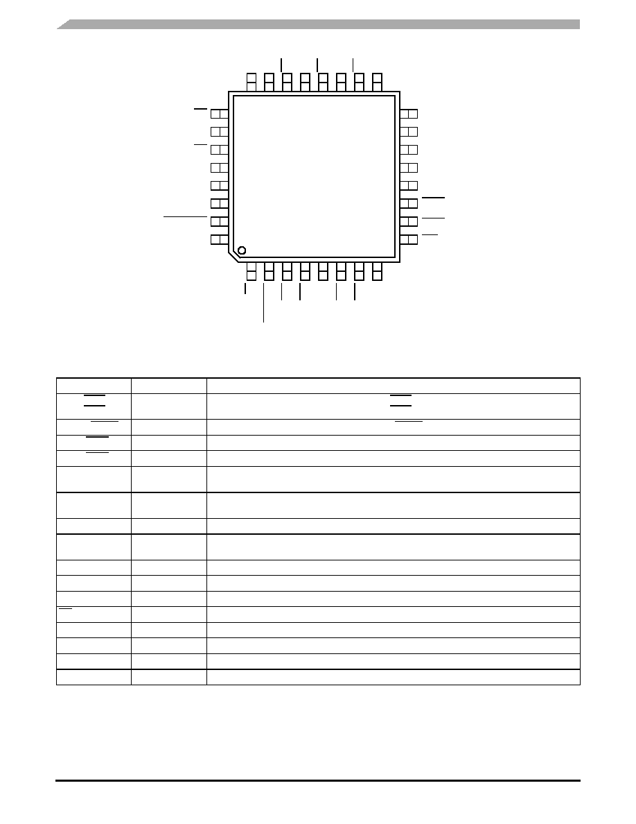
Figure 2. 32-Lead Pinout (Top View)
Table 1. Pin Descriptions
Pin Name
I/O
Pin Definition
CLK0, CLK0
CLK1, CLK1
LVPECL Input
Differential PLL clock reference (CLK0 pulldown, CLK0 pullup)
Differential PLL clock reference (CLK1 pulldown, CLK1 pullup)
Ext_FB, Ext_FB
LVPECL Input
Differential PLL feedback clock (Ext_FB pulldown, Ext_FB pullup)
Qa0:1, Qa0:1
LVPECL Output
Differential 1x output pairs
Qb0:2, Qb0:2
LVPECL Output
Differential 2x output pairs
Inp0bad
LVCMOS Output Indicates detection of a bad input reference clock 0 with respect to the feedback signal. The output is
active HIGH and will remain HIGH until the alarm reset is asserted
Inp1bad
LVCMOS Output Indicates detection of a bad input reference clock 1 with respect to the feedback signal. The output is
active HIGH and will remain HIGH until the alarm reset is asserted
Clk_Selected
LVCMOS Output ‘0' if clock 0 is selected, ‘1' if clock 1 is selected
Alarm_Reset
LVCMOS Input
‘0' will reset the input bad flags and align Clk_Selected with Sel_Clk. The input is “one-shotted”
(50 k
pullup)
Sel_Clk
LVCMOS Input
‘0' selects CLK0, ‘1' selects CLK1 (50 k
pulldown)
Manual_Override
LVCMOS Input
‘1' disables internal clock switch circuitry (50 k
pulldown)
PLL_En
LVCMOS Input
‘0' bypasses selected input reference around the phase-locked loop (50 k
pullup)
MR
LVCMOS Input
‘0' resets the internal dividers forcing Q outputs LOW. Asynchronous to the clock (50 k
pullup)
VCCA
Power Supply
PLL power supply
VCC
Power Supply
Digital power supply
GNDA
Power Supply
PLL ground
GND
Power Supply
Digital ground
Qa1
Qa0
VCC
VCC_PLL
Man_Override
VCC
Inp0bad
Inp1bad
Clk_Selected
GND
Ext_FB
V
CC
Qb
0
Qb
0
Qb
1
Qb
1
Qb
2
Qb
2
V
CC
MR
Ala
rm_
Res
et
CL
K0
CL
K0
Se
l_
Cl
k
CL
K1
CL
K1
GN
D
25
26
27
28
29
30
31
32
15
14
13
12
11
10
9
12
3
4
5
6
78
24
23
22
21
20
19
18
17
16
MPC9993
PLL_EN
Ext_FB
GND
相关PDF资料 |
PDF描述 |
|---|---|
| MPC9993AC | 9993 SERIES, PLL BASED CLOCK DRIVER, 5 TRUE OUTPUT(S), 0 INVERTED OUTPUT(S), PQFP32 |
| MSFLDL-TTL-200 | ACTIVE DELAY LINE, TRUE OUTPUT, SIP4 |
| MSFLDL-TTL-19 | ACTIVE DELAY LINE, TRUE OUTPUT, SIP4 |
| MSFLDL-TTL-21 | ACTIVE DELAY LINE, TRUE OUTPUT, SIP4 |
| MSFLDL-TTL-150 | ACTIVE DELAY LINE, TRUE OUTPUT, SIP4 |
相关代理商/技术参数 |
参数描述 |
|---|---|
| MPC9993D | 制造商:MOTOROLA 制造商全称:Motorola, Inc 功能描述:INTELLIGENT DYNAMIC CLOCK SWITCH (IDCS)PLL CLOCK DRIVER |
| MPC9993DFA | 制造商:MOTOROLA 制造商全称:Motorola, Inc 功能描述:INTELLIGENT DYNAMIC CLOCK SWITCH (IDCS)PLL CLOCK DRIVER |
| MPC9993FA | 功能描述:时钟驱动器及分配 3.3V 200MHz Clock Generator RoHS:否 制造商:Micrel 乘法/除法因子:1:4 输出类型:Differential 最大输出频率:4.2 GHz 电源电压-最大: 电源电压-最小:5 V 最大工作温度:+ 85 C 封装 / 箱体:SOIC-8 封装:Reel |
| MPC99J93 | 制造商:MOTOROLA 制造商全称:Motorola, Inc 功能描述:Intelligent Dynamic Clock Switch (IDCS) PLL Clock Driver |
| MPC99J93AC | 功能描述:时钟驱动器及分配 RoHS:否 制造商:Micrel 乘法/除法因子:1:4 输出类型:Differential 最大输出频率:4.2 GHz 电源电压-最大: 电源电压-最小:5 V 最大工作温度:+ 85 C 封装 / 箱体:SOIC-8 封装:Reel |
发布紧急采购,3分钟左右您将得到回复。