- 您现在的位置:买卖IC网 > PDF目录98030 > MPS6521RL (ON SEMICONDUCTOR) 100 mA, 25 V, NPN, Si, SMALL SIGNAL TRANSISTOR, TO-92 PDF资料下载
参数资料
| 型号: | MPS6521RL |
| 厂商: | ON SEMICONDUCTOR |
| 元件分类: | 小信号晶体管 |
| 英文描述: | 100 mA, 25 V, NPN, Si, SMALL SIGNAL TRANSISTOR, TO-92 |
| 封装: | TO-226AA, 3 PIN |
| 文件页数: | 9/11页 |
| 文件大小: | 480K |
| 代理商: | MPS6521RL |
NPN MPS6521 PNP MPS6523
http://onsemi.com
832
NPN
MPS6521
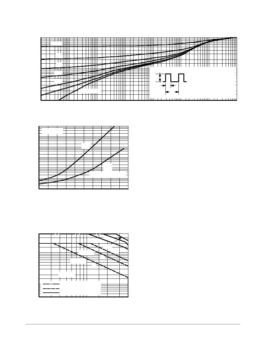
Figure 19. Thermal Response
t, TIME (ms)
1.0
0.01
r(t)
TRANSIENT
THERMAL
RESIST
ANCE
(NORMALIZED)
0.01
0.02
0.03
0.05
0.07
0.1
0.2
0.3
0.5
0.7
0.02
0.05 0.1 0.2
0.5
1.0 2.0
5.0
10
20
50
100 200
500 1.0k 2.0k
5.0k 10k 20k 50k 100k
D = 0.5
0.2
0.1
0.05
0.02
0.01
SINGLE PULSE
DUTY CYCLE, D = t1/t2
D CURVES APPLY FOR POWER
PULSE TRAIN SHOWN
READ TIME AT t1 (SEE AN–569)
ZqJA(t) = r(t) w RqJA
TJ(pk) – TA = P(pk) ZqJA(t)
t1
t2
P(pk)
FIGURE 20
Figure 21.
TJ, JUNCTION TEMPERATURE (°C)
104
-40
I C
,COLLECT
OR
CURRENT
(nA)
Figure 22.
VCE, COLLECTOR-EMITTER VOLTAGE (VOLTS)
400
2.0
I C
,COLLECT
OR
CURRENT
(mA)
DESIGN NOTE: USE OF THERMAL RESPONSE DATA
A train of periodical power pulses can be represented by
the model as shown in Figure 20. Using the model and the de-
vice thermal response the normalized effective transient ther-
mal resistance of Figure 19 was calculated for various duty
cycles.
To find ZθJA(t), multiply the value obtained from Figure 19
by the steady state value RθJA.
Example:
The MPS6521 is dissipating 2.0 watts peak under the follow-
ing conditions:
t1 = 1.0 ms, t2 = 5.0 ms. (D = 0.2)
Using Figure 19 at a pulse width of 1.0 ms and D = 0.2, the
reading of r(t) is 0.22.
The peak rise in junction temperature is therefore
T = r(t) x P(pk) x RθJA = 0.22 x 2.0 x 200 = 88°C.
For more information, see ON Semiconductor Application
Note AN569/D, available from the Literature Distribution
Center or on our website at www.onsemi.com.
The safe operating area curves indicate IC–VCE limits of
the transistor that must be observed for reliable operation.
Collector load lines for specific circuits must fall below the
limits indicated by the applicable curve.
The data of Figure 22 is based upon TJ(pk) = 150°C; TC or
TA is variable depending upon conditions. Pulse curves are
valid for duty cycles to 10% provided TJ(pk) ≤ 150°C. TJ(pk)
may be calculated from the data in Figure 19. At high case or
ambient temperatures, thermal limitations will reduce the
power that can be handled to values less than the limitations
imposed by second breakdown.
10-2
10-1
100
101
102
103
-20
0
+20 +40 +60 +80 +100 +120 +140 +160
VCC = 30 Vdc
ICEO
ICBO
AND
ICEX @ VBE(off) = 3.0 Vdc
TA = 25°C
CURRENT LIMIT
THERMAL LIMIT
SECOND BREAKDOWN LIMIT
1.0 ms
10 s
TC = 25°C
1.0 s
dc
4.0
6.0
10
20
40
60
100
200
4.0
6.0 8.0 10
20
40
TJ = 150°C
100 s
相关PDF资料 |
PDF描述 |
|---|---|
| MPS6521RLRM | 100 mA, 25 V, NPN, Si, SMALL SIGNAL TRANSISTOR, TO-92 |
| MPS6523RLRM | 100 mA, 25 V, PNP, Si, SMALL SIGNAL TRANSISTOR, TO-92 |
| MPS6523RLRA | 100 mA, 25 V, PNP, Si, SMALL SIGNAL TRANSISTOR, TO-92 |
| MPS6521RL1 | 100 mA, 25 V, NPN, Si, SMALL SIGNAL TRANSISTOR, TO-92 |
| MPS6523RL | 100 mA, 25 V, PNP, Si, SMALL SIGNAL TRANSISTOR, TO-92 |
相关代理商/技术参数 |
参数描述 |
|---|---|
| MPS6521RLRA | 功能描述:两极晶体管 - BJT 100mA 40V NPN RoHS:否 制造商:STMicroelectronics 配置: 晶体管极性:PNP 集电极—基极电压 VCBO: 集电极—发射极最大电压 VCEO:- 40 V 发射极 - 基极电压 VEBO:- 6 V 集电极—射极饱和电压: 最大直流电集电极电流: 增益带宽产品fT: 直流集电极/Base Gain hfe Min:100 A 最大工作温度: 安装风格:SMD/SMT 封装 / 箱体:PowerFLAT 2 x 2 |
| MPS6521RLRAG | 功能描述:两极晶体管 - BJT 100mA 40V NPN RoHS:否 制造商:STMicroelectronics 配置: 晶体管极性:PNP 集电极—基极电压 VCBO: 集电极—发射极最大电压 VCEO:- 40 V 发射极 - 基极电压 VEBO:- 6 V 集电极—射极饱和电压: 最大直流电集电极电流: 增益带宽产品fT: 直流集电极/Base Gain hfe Min:100 A 最大工作温度: 安装风格:SMD/SMT 封装 / 箱体:PowerFLAT 2 x 2 |
| MPS6522 | 功能描述:两极晶体管 - BJT PNP Gen Pur SS RoHS:否 制造商:STMicroelectronics 配置: 晶体管极性:PNP 集电极—基极电压 VCBO: 集电极—发射极最大电压 VCEO:- 40 V 发射极 - 基极电压 VEBO:- 6 V 集电极—射极饱和电压: 最大直流电集电极电流: 增益带宽产品fT: 直流集电极/Base Gain hfe Min:100 A 最大工作温度: 安装风格:SMD/SMT 封装 / 箱体:PowerFLAT 2 x 2 |
| MPS6523 | 功能描述:两极晶体管 - BJT PNP Transistor General Purpose RoHS:否 制造商:STMicroelectronics 配置: 晶体管极性:PNP 集电极—基极电压 VCBO: 集电极—发射极最大电压 VCEO:- 40 V 发射极 - 基极电压 VEBO:- 6 V 集电极—射极饱和电压: 最大直流电集电极电流: 增益带宽产品fT: 直流集电极/Base Gain hfe Min:100 A 最大工作温度: 安装风格:SMD/SMT 封装 / 箱体:PowerFLAT 2 x 2 |
| MPS6523_01 | 制造商:FAIRCHILD 制造商全称:Fairchild Semiconductor 功能描述:PNP General Purpose Amplifier |
发布紧急采购,3分钟左右您将得到回复。