- 您现在的位置:买卖IC网 > PDF目录371140 > MPX2202D (MOTOROLA INC) Sensor PDF资料下载
参数资料
| 型号: | MPX2202D |
| 厂商: | MOTOROLA INC |
| 元件分类: | 压力传感器 |
| 英文描述: | Sensor |
| 中文描述: | DIFFERENTIAL, PEIZORESISTIVE PRESSURE SENSOR, 0-14.5Psi, 0.4%, 0-40mV, ROUND, THROUGH HOLE MOUNT |
| 封装: | UNIBODY PACKAGE-4 |
| 文件页数: | 496/670页 |
| 文件大小: | 6375K |
| 代理商: | MPX2202D |
第1页第2页第3页第4页第5页第6页第7页第8页第9页第10页第11页第12页第13页第14页第15页第16页第17页第18页第19页第20页第21页第22页第23页第24页第25页第26页第27页第28页第29页第30页第31页第32页第33页第34页第35页第36页第37页第38页第39页第40页第41页第42页第43页第44页第45页第46页第47页第48页第49页第50页第51页第52页第53页第54页第55页第56页第57页第58页第59页第60页第61页第62页第63页第64页第65页第66页第67页第68页第69页第70页第71页第72页第73页第74页第75页第76页第77页第78页第79页第80页第81页第82页第83页第84页第85页第86页第87页第88页第89页第90页第91页第92页第93页第94页第95页第96页第97页第98页第99页第100页第101页第102页第103页第104页第105页第106页第107页第108页第109页第110页第111页第112页第113页第114页第115页第116页第117页第118页第119页第120页第121页第122页第123页第124页第125页第126页第127页第128页第129页第130页第131页第132页第133页第134页第135页第136页第137页第138页第139页第140页第141页第142页第143页第144页第145页第146页第147页第148页第149页第150页第151页第152页第153页第154页第155页第156页第157页第158页第159页第160页第161页第162页第163页第164页第165页第166页第167页第168页第169页第170页第171页第172页第173页第174页第175页第176页第177页第178页第179页第180页第181页第182页第183页第184页第185页第186页第187页第188页第189页第190页第191页第192页第193页第194页第195页第196页第197页第198页第199页第200页第201页第202页第203页第204页第205页第206页第207页第208页第209页第210页第211页第212页第213页第214页第215页第216页第217页第218页第219页第220页第221页第222页第223页第224页第225页第226页第227页第228页第229页第230页第231页第232页第233页第234页第235页第236页第237页第238页第239页第240页第241页第242页第243页第244页第245页第246页第247页第248页第249页第250页第251页第252页第253页第254页第255页第256页第257页第258页第259页第260页第261页第262页第263页第264页第265页第266页第267页第268页第269页第270页第271页第272页第273页第274页第275页第276页第277页第278页第279页第280页第281页第282页第283页第284页第285页第286页第287页第288页第289页第290页第291页第292页第293页第294页第295页第296页第297页第298页第299页第300页第301页第302页第303页第304页第305页第306页第307页第308页第309页第310页第311页第312页第313页第314页第315页第316页第317页第318页第319页第320页第321页第322页第323页第324页第325页第326页第327页第328页第329页第330页第331页第332页第333页第334页第335页第336页第337页第338页第339页第340页第341页第342页第343页第344页第345页第346页第347页第348页第349页第350页第351页第352页第353页第354页第355页第356页第357页第358页第359页第360页第361页第362页第363页第364页第365页第366页第367页第368页第369页第370页第371页第372页第373页第374页第375页第376页第377页第378页第379页第380页第381页第382页第383页第384页第385页第386页第387页第388页第389页第390页第391页第392页第393页第394页第395页第396页第397页第398页第399页第400页第401页第402页第403页第404页第405页第406页第407页第408页第409页第410页第411页第412页第413页第414页第415页第416页第417页第418页第419页第420页第421页第422页第423页第424页第425页第426页第427页第428页第429页第430页第431页第432页第433页第434页第435页第436页第437页第438页第439页第440页第441页第442页第443页第444页第445页第446页第447页第448页第449页第450页第451页第452页第453页第454页第455页第456页第457页第458页第459页第460页第461页第462页第463页第464页第465页第466页第467页第468页第469页第470页第471页第472页第473页第474页第475页第476页第477页第478页第479页第480页第481页第482页第483页第484页第485页第486页第487页第488页第489页第490页第491页第492页第493页第494页第495页当前第496页第497页第498页第499页第500页第501页第502页第503页第504页第505页第506页第507页第508页第509页第510页第511页第512页第513页第514页第515页第516页第517页第518页第519页第520页第521页第522页第523页第524页第525页第526页第527页第528页第529页第530页第531页第532页第533页第534页第535页第536页第537页第538页第539页第540页第541页第542页第543页第544页第545页第546页第547页第548页第549页第550页第551页第552页第553页第554页第555页第556页第557页第558页第559页第560页第561页第562页第563页第564页第565页第566页第567页第568页第569页第570页第571页第572页第573页第574页第575页第576页第577页第578页第579页第580页第581页第582页第583页第584页第585页第586页第587页第588页第589页第590页第591页第592页第593页第594页第595页第596页第597页第598页第599页第600页第601页第602页第603页第604页第605页第606页第607页第608页第609页第610页第611页第612页第613页第614页第615页第616页第617页第618页第619页第620页第621页第622页第623页第624页第625页第626页第627页第628页第629页第630页第631页第632页第633页第634页第635页第636页第637页第638页第639页第640页第641页第642页第643页第644页第645页第646页第647页第648页第649页第650页第651页第652页第653页第654页第655页第656页第657页第658页第659页第660页第661页第662页第663页第664页第665页第666页第667页第668页第669页第670页
3–350
Motorola Sensor Device Data
For More Information On This Product,
Go to: www.freescale.com
Summarizing (through Step 4), the calculations are based
on a minimum desired resolution. The resolution requirement
determines the number of steps or “pieces” into which the
signal must be broken. This number of steps or “pieces”
multiplied by the number of millivolts per step equals a
minimum voltage range which is defined as the Minimum
Required Span. Finally to ensure that this Minimum Required
Span is achieved over the entire distribution of sensor spans,
the gain is calculated using the worst case smallest sensor
span.
Note:The gain also will have variation due to resistor
tolerances in the amplifier circuit. To ensure that the system
variation due to resistor tolerances is negligible when
compared to other sources of variation, the system should be
designed using resistors with tolerances of 1% or better.
5. Calculate the worst case Maximum Span. The Maximum
Span is the largest possible span and is calculated using
the maximum full–scale sensor voltage span, MaxFSS,
and the Gain. The worst case maximum full–scale sensor
span occurs at the coldest temperature, MinTemp. After
calculating the Maximum Span, the remaining dynamic
range within the A/D’s window or saturation levels of the
amplifier is the smallest number of “bits” (most limiting
case) available for headroom.
Maximum Span =
[Gain]
[MaxFSS]
[1 + TCVFSS
(MinTemp – 25)]
The term [1 + TCVFSS
(MinTemp – 25)] is the temperature
effect on the span.
The Maximum Span calculated from the above equation is
depicted in Figure 4.
6. Calculate the Calculated Headroom. The Calculated
Headroom is a subset of the general term “headroom”
because it reserves “bits” in the A/D’s dynamic range only
for the sources of variation from the sensor’s zero–pres-
sure offset voltage. Headroom, in general, is reserved for
all sources of variation: system components, resistor
tolerances (if significant), and the sensor. However, the
largest part of the “headroom” must be reserved for the
device–to–device variations and temperature effects on
the sensor’s zero–pressure offset voltage. Therefore, the
sources of variation from the other system components
are subtracted immediately from the headroom so that
the focus can be on the sensor–related variations (refer
to Figure 5 and the following equation for the Calculated
Headroom). For these design examples, the supply is a
single, regulated 5 V
±
5% supply (the regulator’s
tolerance is referred to as Vtol). An assumption for a
typical rail–to–rail op–amp’s saturation levels (referred to
as Vlo and Vhi) is 0.2 V above the low supply rail (ground)
and 0.2 V below the high supply rail (5 V). Additionally,
the worst case (smallest) supply voltage is 5 V – 5% or
4.75 V.
Calculated Headroom
·
Vlo– Maximum Span
The preceding equation assumes that the difference
between Vhi and the high supply rail (or high reference of an
A/D) is equal to the difference between Vlo and the low supply
rail (or low reference of an A/D); thus the term (2
Vlo).
5
·
(1–100) – 2
VS’s NOMINAL VALUE
(NOT INCLUDING Vtol)
VS (INCLUDING Vtol) AND
A/D HIGH REFERENCE
HIGH SAT. LEVEL
OF AMPLIFIER
FULL–SCALE
OUTPUT VOLTAGE
ZERO PRESSURE
OFFSET VOLTAGE
LOW SAT. LEVEL
OF AMPLIFIER
GROUND AND A/D
LOW REFERENCE
MAXIMUM
SPAN
CALCULATED
HEADROOM
AMPLIFIER’S
DYNAMIC
RANGE
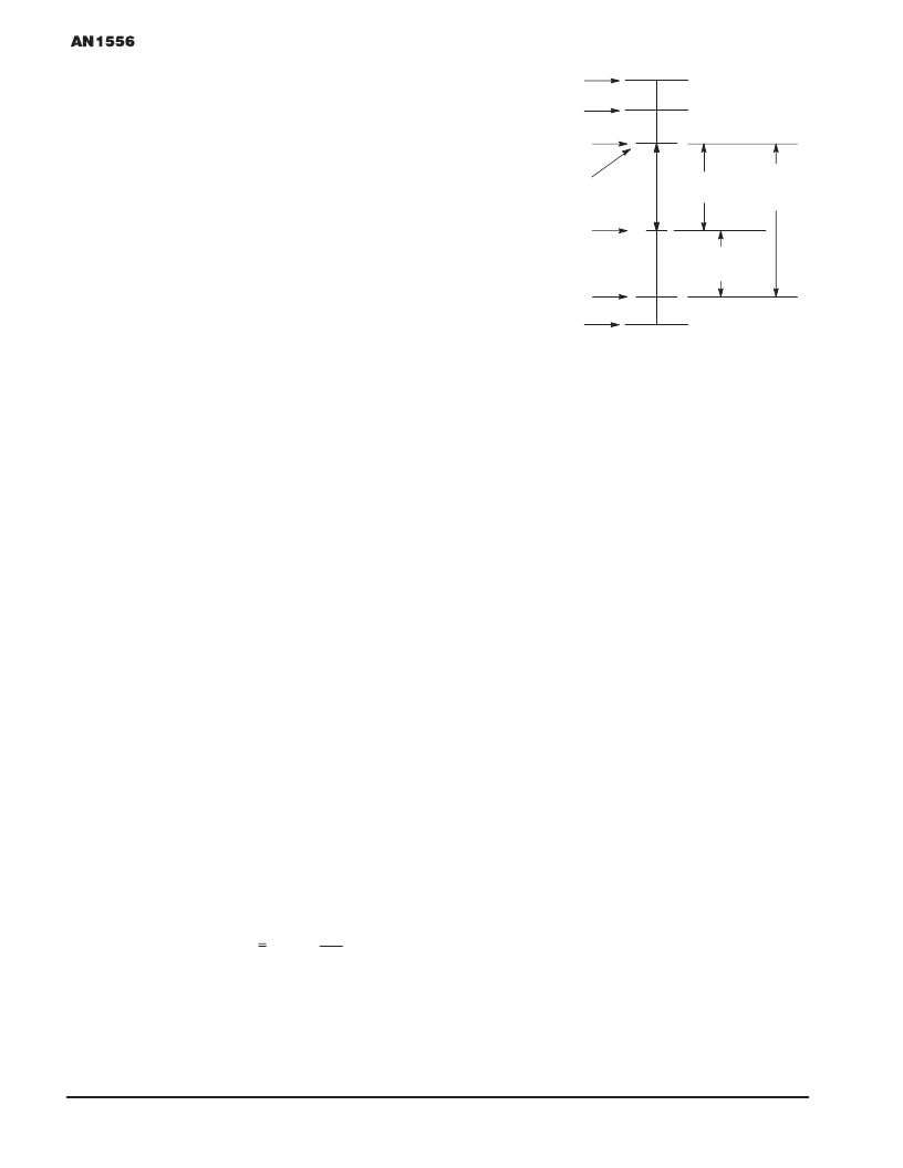
Figure 5. From Ground to VS, a Section of Voltage Is
Reserved for Each Source of Variation
Step 6 is considered a pivotal step because it transitions the
methodology’s calculations from the performance require-
ments to the headroom requirements. Up to Step 6, the
methodology considered only the span of the sensor to
guarantee a minimum resolution despite device–to–device
variation, component tolerances, and temperature effects.
Upon calculating the Calculated Headroom, the remaining
steps of the methodology that are detailed below consider the
offset variations (due to device–to–device and temperature).
These offset variations are added together to comprise what
is defined as the Required Headroom which is the required
number of “bits” in the A/D’s dynamic range needed to
accommodate the offset variations. This Required Headroom
is then compared to the Calculated Headroom (from the
preceding calculation) to determine if the Calculated Head-
room is sufficient to allow for the offset variations (i.e., the
Calculated Headroom must be greater than or equal to the
Required Headroom). In the case that the Calculated Head-
room is not sufficiently large, relaxing the resolution require-
ment or reducing, if possible, the variation of either offset,
span, component tolerances, or a combination of all three is
required.
7. Calculate the maximum offset drift due to temperature
fluctuations (defined as the Maximum Temperature Effect
on Offset). A conservative approach to this calculation is
to determine the maximum total voltage change of offset
over the application’s entire operating temperature range.
This maximum change of offset is the product of the Gain,
TCVoff, and the application’s entire operating temperature
range (from Maxtemp to MinTemp). Since the tempera-
ture coefficient of offset can be positive or negative, the
offset may increase or decrease with increasing tempera-
ture and, likewise, for decreasing temperature. Though
this step only considers the maximum magnitude of the
change in offset due to temperature, a segment in the
Required Headroom is reserved for both possibilities of a
positive or negative temperature coefficient of offset (see
Figure 6). The sign (positive or negative) of the total offset
change due to temperature is also considered in upcom-
ing steps.
F
Freescale Semiconductor, Inc.
n
.
相关PDF资料 |
PDF描述 |
|---|---|
| MPXV5010DP | Sensor |
| MPXV5010G6U | Sensor |
| MPXV5010G7U | Sensor |
| MPXV5010GC6T1 | Sensor |
| MPXV5010GC6U | Sensor |
相关代理商/技术参数 |
参数描述 |
|---|---|
| MPX2202D | 制造商:Freescale Semiconductor 功能描述:Pressure Sensor IC Package/Case:CASE 344 |
| MPX2202DP | 功能描述:板上安装压力/力传感器 UNIBODY COMPENSATED RoHS:否 制造商:Honeywell 工作压力:0 bar to 4 bar 压力类型:Gage 准确性:+ / - 0.25 % 输出类型:Digital 安装风格:Through Hole 工作电源电压:5 V 封装 / 箱体:SIP 端口类型:Dual Radial Barbed, Same sides |
| MPX2202DP | 制造商:Freescale Semiconductor 功能描述:Pressure Sensor IC Package/Case:CASE 135 |
| MPX2202GP | 功能描述:板上安装压力/力传感器 UNIBODY COMPENSATED RoHS:否 制造商:Honeywell 工作压力:0 bar to 4 bar 压力类型:Gage 准确性:+ / - 0.25 % 输出类型:Digital 安装风格:Through Hole 工作电源电压:5 V 封装 / 箱体:SIP 端口类型:Dual Radial Barbed, Same sides |
| MPX2202GP | 制造商:Freescale Semiconductor 功能描述:IC PRESSURE SENSOR GAUGE 29 PSI 制造商:Freescale Semiconductor 功能描述:IC, PRESSURE SENSOR, GAUGE, 29 PSI |
发布紧急采购,3分钟左右您将得到回复。