- 您现在的位置:买卖IC网 > PDF目录296638 > MSK5940-5.2RHTD (MS KENNEDY CORP) 5.2 V FIXED NEGATIVE LDO REGULATOR, 1.2 V DROPOUT, SFM3 PDF资料下载
参数资料
| 型号: | MSK5940-5.2RHTD |
| 厂商: | MS KENNEDY CORP |
| 元件分类: | 固定负电压单路输出LDO稳压器 |
| 英文描述: | 5.2 V FIXED NEGATIVE LDO REGULATOR, 1.2 V DROPOUT, SFM3 |
| 封装: | BEND DOWN, SIP-3 |
| 文件页数: | 2/6页 |
| 文件大小: | 284K |
| 代理商: | MSK5940-5.2RHTD |
%
V
%
mA
A
dB
°C/W
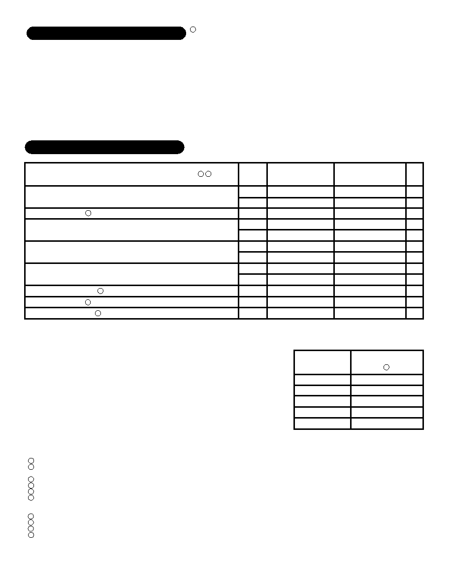
PART
NUMBER
Dropout Voltage
Short Circuit Current
Ripple Rejection
Thermal Resistance
Max.
1.0
2.0
1.0
2.0
0.5
0.75
10
-
7.2
Storage Temperature Range
Lead Temperature Range
(10 Seconds)
Case Operating Temperature
MSK 5940K/H/E RH
MSK 5940RH
-35V
-30V
Internally Limited
-3A
+150°C
-2V
-65°C to +150°C
300°C
-55°C to +125°C
-40°C to +85°C
ABSOLUTE MAXIMUM RATINGS
TST
TLD
TC
Input Voltage
Input Voltage (WRT VOUT)
Power Dissipation
Output Current
Junction Temperature
Output Reverse Voltage
○○○○○○○○
○○○○
○○○○○○
-VIN
PD
IOUT
TJ
IOUT
○○○○○○○○○○
○
○○○○
○○○○○○○○○○○○
○○○○
○○○○○○
○○○○
○
Output is decoupled to ground using 33F minimum, low ESR capacitors unless otherwise specified.
Guaranteed by design but not tested. Typical parameters are representative of actual device
performance but are for reference only.
All output parameters are tested using a low duty cycle pulse to maintain TJ = TC.
Industrial grade and "E" suffix devices shall be tested to subgroup 1 unless otherwise specified.
Military grade devices ("H" and "K" suffix) shall be 100% tested to subgroups 1,2 and 3.
Subgroup 1
TA=TC=+25°C
2
TA=TC=+125°C
3
TA=TC=-55°C
Please consult the factory if alternate output voltages are required.
Input voltage (VIN= VOUT + a specified voltage) is implied to be more negative than VOUT.
Continuous operation at or above absolute maximum ratings may adversely effect the device performance and/or life cycle.
All parameter limits are pre-irradiation. Radiation performace is not yet characterized.
Min.
-
3.0
60
-
Group A
Subgroup
1
2,3
1
2,3
1
2,3
1
2,3
-
Min.
-
3.0
60
-
Typ.
0.1
0.7
0.2
0.3
0.1
0.2
4.5
3.5
75
7.0
Typ.
0.1
-
0.8
0.2
-
0.1
-
4.5
-
3.5
75
7.0
Max.
2.0
-
1.2
2.0
-
0.6
-
12
-
7.5
Parameter
ELECTRICAL SPECIFICATIONS
Test Conditions
Units
MSK 5940RH
MSK 5940K/H/E RH
3
2
0A≤IOUT≤3A; VOUT=1%
10mA≤IOUT≤3A
VIN=VOUT+3V
IOUT=10mA
(VOUT+3V)≤VIN≤(VOUT+15V)
VIN=VOUT+5V
IOUT=3A; COUT=25F; f=120Hz
JUNCTION TO CASE @ 125°C
-5.0V
-5.2V
-10.0V
-12.0V
-15.0V
MSK5940-5.0RH
MSK5940-5.2RH
MSK5940-10RH
MSK5940-12RH
MSK5940-15RH
OUTPUT VOLTAGE
7
2
1
2
3
4
5
6
7
8
9
10
2
NOTES:
○○
Output Voltage Tolerance
Load Regulation
Line Regulation
IOUT=10mA; VIN=VOUT+3V
Quiescent Current
VIN=VOUT+3V; IOUT=10mA
2
PRELIMINARY Rev. C 6/08
○○○○○○○
○
○○○○○○
○○○○○
10
9
相关PDF资料 |
PDF描述 |
|---|---|
| MSK5940-5.2RHTS | 5.2 V FIXED NEGATIVE LDO REGULATOR, 1.2 V DROPOUT, SFM3 |
| MSK5940-5.2RHTU | 5.2 V FIXED NEGATIVE LDO REGULATOR, 1.2 V DROPOUT, SFM3 |
| MSM11000WXLMB-45 | 1M X 1 STANDARD SRAM, 45 ns, CQCC32 |
| MSM11000VMB-45 | 1M X 1 STANDARD SRAM, 45 ns, CDXA28 |
| MSM11000GI-45 | 1M X 1 STANDARD SRAM, 45 ns, CDFP28 |
相关代理商/技术参数 |
参数描述 |
|---|---|
| MSK600 | 制造商:MSK 制造商全称:M.S. Kennedy Corporation 功能描述:WIDE BANDWIDTH HIGH VOLTAGE AMPLIFIER |
| MSK601 | 制造商:MSK 制造商全称:M.S. Kennedy Corporation 功能描述:WIDE BANDWIDTH HIGH VOLTAGE AMPLIFIER |
| MSK601B | 制造商:MSK 制造商全称:M.S. Kennedy Corporation 功能描述:WIDE BANDWIDTH HIGH VOLTAGE AMPLIFIER |
| MSK604 | 制造商:MSK 制造商全称:M.S. Kennedy Corporation 功能描述:NEGATIVE OUTPUT WIDE BANDWIDTH HIGH VOLTAGE AMPLIFIER |
| MSK604B | 制造商:MSK 制造商全称:M.S. Kennedy Corporation 功能描述:NEGATIVE OUTPUT WIDE BANDWIDTH HIGH VOLTAGE AMPLIFIER |
发布紧急采购,3分钟左右您将得到回复。