- 您现在的位置:买卖IC网 > PDF目录264435 > MSP5.0A-M3/89A (VISHAY SEMICONDUCTORS) 100 W, UNIDIRECTIONAL, SILICON, TVS DIODE PDF资料下载
参数资料
| 型号: | MSP5.0A-M3/89A |
| 厂商: | VISHAY SEMICONDUCTORS |
| 元件分类: | 参考电压二极管 |
| 英文描述: | 100 W, UNIDIRECTIONAL, SILICON, TVS DIODE |
| 封装: | HALOGEN FREE AND ROHS COMPLIANT, PLASTIC, MICROSMP, 2 PIN |
| 文件页数: | 1/4页 |
| 文件大小: | 84K |
| 代理商: | MSP5.0A-M3/89A |
Document Number: 88487
For technical questions within your region, please contact one of the following:
www.vishay.com
Revision: 19-Apr-11
DiodesAmericas@vishay.com, DiodesAsia@vishay.com, DiodesEurope@vishay.com
23
This document is subject to change without notice.
THE PRODUCTS DESCRIBED HEREIN AND THIS DOCUMENT ARE SUBJECT TO SPECIFIC DISCLAIMERS, SET FORTH AT www.vishay.com/doc?91000
Surface Mount TRANSZORB Transient Voltage Suppressors
MSP5.0A
Vishay General Semiconductor
New Product
TYPICAL APPLICATIONS
Use in sensitive electronics protection against voltage
transients induced by inductive load switching and lighting
on ICs, MOSFET, signal lines of sensor units specifically for
protecting 5.0 V supplied sensitive equipment against
transient overvoltages.
FEATURES
Very low profile - typical height of 0.65 mm
Ideal for automated placement
Oxide planar chip junction
Uni-directional polarity only
Peak pulse power: 100 W (10/1000 μs)
ESD capability: 15 kV (air), 8 kV (contact)
Meets MSL level 1, per J-STD-020C, LF maximum peak of
260 °C
AEC-Q101 qualified
Compliant
to
RoHS
Directive
2002/95/EC
and
in
accordance to WEEE 2002/96/EC
Halogen-free according to IEC 61249-2-21 definition
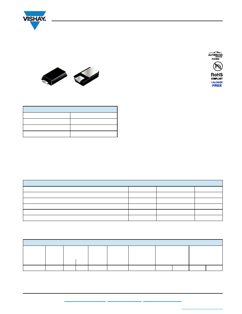
MECHANICAL DATA
Case: MicroSMP
Molding compound meets UL 94 V-0 flammability rating
Base P/N-M3 - halogen-free, RoHS compliant, and
commercial grade
Base P/NHM3 - halogen-free, RoHS compliant, and
automotive grade
Terminals:
Matte
tin
plated
leads,
solderable
per
J-STD-002 and JESD 22-B102
M3 suffix meets JESD 201 class 1A whisker test, HM3 suffix
meets JESD 201 class 2 whisker test
Polarity: Color band denotes the cathode end
Notes
(1) Non-repetitive current pulse, per fig. 1
(2) Mounted on 6.0 mm x 6.0 mm copper pads to each terminal
Notes
(1) Pulse test: tp 50 ms
(2) Surge current waveform per fig. 1 and derate per fig. 2
PRIMARY CHARACTERISTICS
VWM
5.0 V
PPPM
100 W
IFSM
25 A
TJ max.
150 °C
MicroSMP
eSMP Series
Top View
Bottom View
MAXIMUM RATINGS (TA = 25 °C unless otherwise noted)
PARAMETER
SYMBOL
VALUE
UNIT
Peak pulse power dissipation
PPPM (1)(2)
100
W
Peak pulse current with a 10/1000 μs waveform (fig. 1)
IPPM
10.9
A
Non repetitive peak forward surge current 10 ms single half sine-wave
IFSM (2)
25
A
Power dissipation TL = 120 °C
PD (2)
1.0
W
Operating junction and storage temperature range
TJ, TSTG
- 55 to + 150
°C
ELECTRICAL CHARACTERISTICS (TA = 25 °C unless otherwise noted)
DEVICE
TYPE
DEVICE
MARKING
CODE
BREAKDOWN
VOLTAGE
VBR AT IT (V) (1)
TEST
CURRENT
IT
(mA)
STAND-OFF
VOLTAGE
VWM
(V)
MAX. REVERSE
LEAKAGE
AT VWM
ID ( A)
MAX. CLAMPING
VOLTAGE (2)
VC (V) AT IPPM (A)
10/1000 s
MAX. CLAMPING
VOLTAGE (2)
VC (V) AT IPPM (A)
8/20 s
MIN.
MAX.
MSP5.0A
AE
6.40
7.07
10
5.0
100
9.2
10.9
14.5
57
相关PDF资料 |
PDF描述 |
|---|---|
| MIV41012-21 | mm WAVE BAND, 0.4 pF, 75 V, SILICON, VARIABLE CAPACITANCE DIODE |
| MA46476-134 | VHF-KA BAND, 2 pF, 22 V, GALLIUM ARSENIDE, HYPERABRUPT VARIABLE CAPACITANCE DIODE |
| MA4E2054B1-287T | SILICON, LOW BARRIER SCHOTTKY, MIXER DIODE |
| MQ15KP100CA | 15000 W, BIDIRECTIONAL, SILICON, TVS DIODE, DO-204AR |
| MQ15KP110CAE3TR | 15000 W, BIDIRECTIONAL, SILICON, TVS DIODE, DO-204AR |
相关代理商/技术参数 |
参数描述 |
|---|---|
| MSP50A-M389A | 制造商:VISHAY 制造商全称:Vishay Siliconix 功能描述:Surface Mount TRANSZORB Transient Voltage Suppressors |
| MSP50C30 | 制造商:TI 制造商全称:Texas Instruments 功能描述:MIXED-SIGNAL PROCESSOR |
| MSP50C30PJM | 制造商:TI 制造商全称:Texas Instruments 功能描述:MIXED-SIGNAL PROCESSOR |
| MSP50C32 | 制造商:未知厂家 制造商全称:未知厂家 功能描述:Mixed-Signal Processors |
| MSP50C32N | 制造商:未知厂家 制造商全称:未知厂家 功能描述:Speech Synthesizer |
发布紧急采购,3分钟左右您将得到回复。