- 您现在的位置:买卖IC网 > PDF目录98045 > MTB52N06VT4 (ON SEMICONDUCTOR) 52 A, 60 V, 0.022 ohm, N-CHANNEL, Si, POWER, MOSFET PDF资料下载
参数资料
| 型号: | MTB52N06VT4 |
| 厂商: | ON SEMICONDUCTOR |
| 元件分类: | JFETs |
| 英文描述: | 52 A, 60 V, 0.022 ohm, N-CHANNEL, Si, POWER, MOSFET |
| 封装: | D2PAK-3 |
| 文件页数: | 8/12页 |
| 文件大小: | 114K |
| 代理商: | MTB52N06VT4 |
MTB52N06V
http://onsemi.com
5
VDS
,DRAIN-T
O-SOURCE
VOL
TAGE
(VOL
TS)
V GS
,GA
TE-T
O-SOURCE
VOL
TAGE
(VOL
TS)
DRAIN–TO–SOURCE DIODE CHARACTERISTICS
VSD, SOURCE-TO-DRAIN VOLTAGE (VOLTS)
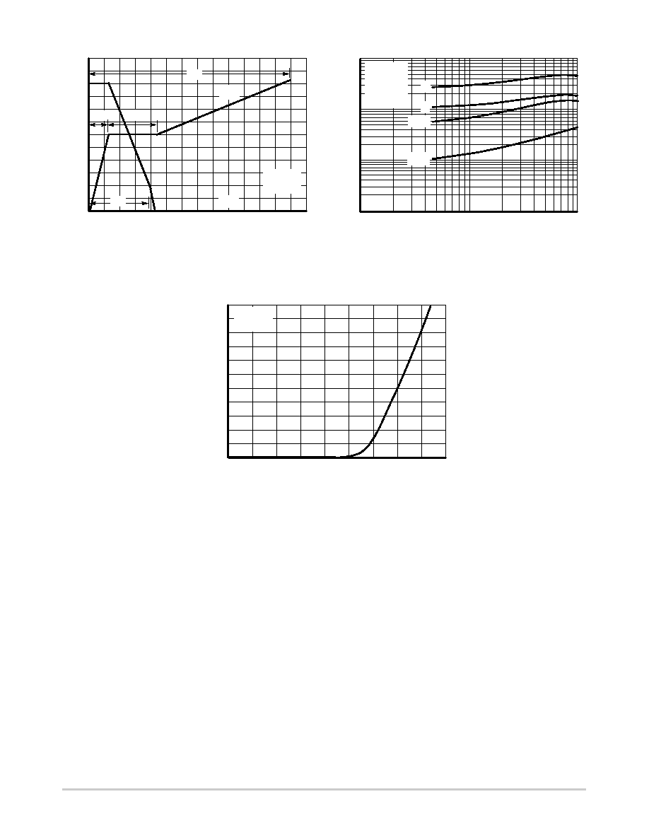
Figure 8. Gate–To–Source and Drain–To–Source
Voltage versus Total Charge
I S
,SOURCE
CURRENT
(AMPS)
Figure 9. Resistive Switching Time
Variation versus Gate Resistance
RG, GATE RESISTANCE (OHMS)
1
10
100
t,TIME
(ns)
VDD = 30 V
ID = 52 A
VGS = 10 V
TJ = 25°C
Figure 10. Diode Forward Voltage versus Current
0
QT, TOTAL CHARGE (nC)
20
40
60
80
140
ID = 52 A
TJ = 25°C
1000
100
10
1
12
6
2
0
8
4
36
33
27
24
6
3
0
QT
Q2
Q1
Q3
VGS
VDS
td(on)
td(off)
tf
tr
VGS = 0 V
TJ = 25°C
50
40
30
20
10
0
0.5
0.6
0.7
0.8
0.9
1
10
30
1.1
100
120
21
18
15
12
9
55
45
35
25
15
5
0.4
0.3
0.2
SAFE OPERATING AREA
The Forward Biased Safe Operating Area curves define
the maximum simultaneous drain–to–source voltage and
drain current that a transistor can handle safely when it is
forward biased. Curves are based upon maximum peak
junction temperature and a case temperature (TC) of 25°C.
Peak repetitive pulsed power limits are determined by using
the thermal response data in conjunction with the procedures
discussed
in
AN569,
“Transient
Thermal
Resistance–General Data and Its Use.”
Switching between the off–state and the on–state may
traverse any load line provided neither rated peak current
(IDM) nor rated voltage (VDSS) is exceeded and the
transition time (tr,tf) do not exceed 10 s. In addition the total
power averaged over a complete switching cycle must not
exceed (TJ(MAX) – TC)/(R
θJC).
A Power MOSFET designated E–FET can be safely used
in switching circuits with unclamped inductive loads. For
reliable operation, the stored energy from circuit inductance
dissipated in the transistor while in avalanche must be less
than the rated limit and adjusted for operating conditions
differing from those specified. Although industry practice is
to rate in terms of energy, avalanche energy capability is not
a constant. The energy rating decreases non–linearly with an
increase of peak current in avalanche and peak junction
temperature.
Although many E–FETs can withstand the stress of
drain–to–source avalanche at currents up to rated pulsed
current (IDM), the energy rating is specified at rated
continuous current (ID), in accordance with industry
custom. The energy rating must be derated for temperature
as shown in the accompanying graph (Figure 12). Maximum
energy at currents below rated continuous ID can safely be
assumed to equal the values indicated.
相关PDF资料 |
PDF描述 |
|---|---|
| MTB60N05HDT4 | 60 A, 50 V, 0.014 ohm, N-CHANNEL, Si, POWER, MOSFET |
| MTB60N05HD | 60 A, 50 V, 0.014 ohm, N-CHANNEL, Si, POWER, MOSFET |
| MTB60N05HDL | 60 A, 50 V, 0.014 ohm, N-CHANNEL, Si, POWER, MOSFET |
| MTB60N05HDG | 60 A, 50 V, 0.014 ohm, N-CHANNEL, Si, POWER, MOSFET |
| MTB60N05HDLT4 | 60 A, 50 V, 0.014 ohm, N-CHANNEL, Si, POWER, MOSFET |
相关代理商/技术参数 |
参数描述 |
|---|---|
| MTB55N03N3 | 制造商:CYSTEKEC 制造商全称:Cystech Electonics Corp. 功能描述:30V N-Channel Logic Level Enhancement Mode MOSFET |
| MTB55N06Z | 制造商:Rochester Electronics LLC 功能描述:- Bulk 制造商:ON Semiconductor 功能描述: |
| MTB55N06ZT4 | 制造商:Rochester Electronics LLC 功能描述:- Bulk |
| MTB55N10Q8 | 制造商:CYSTEKEC 制造商全称:Cystech Electonics Corp. 功能描述:N -Channel Logic Level Enhancement Mode Power MOSFET |
| MTB-5PH002-01 | 制造商:ITT Interconnect Solutions 功能描述:MTB-5PH002-01 - Bulk |
发布紧急采购,3分钟左右您将得到回复。