- 您现在的位置:买卖IC网 > PDF目录96113 > MWT-H971 (MICROWAVE TECHNOLOGY INC) K BAND, GaAs, RF POWER, HEMFET PDF资料下载
参数资料
| 型号: | MWT-H971 |
| 厂商: | MICROWAVE TECHNOLOGY INC |
| 元件分类: | 功率晶体管 |
| 英文描述: | K BAND, GaAs, RF POWER, HEMFET |
| 封装: | HERMETIC SEALED PACKAGE-2 |
| 文件页数: | 2/2页 |
| 文件大小: | 95K |
| 代理商: | MWT-H971 |
4268 Solar Way
Fremont
California 94538 Phone: (510) 651-6700 Fax: (510) 651-2208
4268 Solar Way
Fremont
California 94538 Phone: (510) 651-6700 Fax: (510) 651-2208
All rights reserved. MicroWave Technology, Inc. All specifications subject to change without notice.
75
°°°°°C or Lower
100
125
75
°°°°°C or Lower
100
125
150
0
2
4
6
8
400
325
250
175
100
0
Vds (V)
Ids
(mA)
Absolute Maximum Continuous Maximum
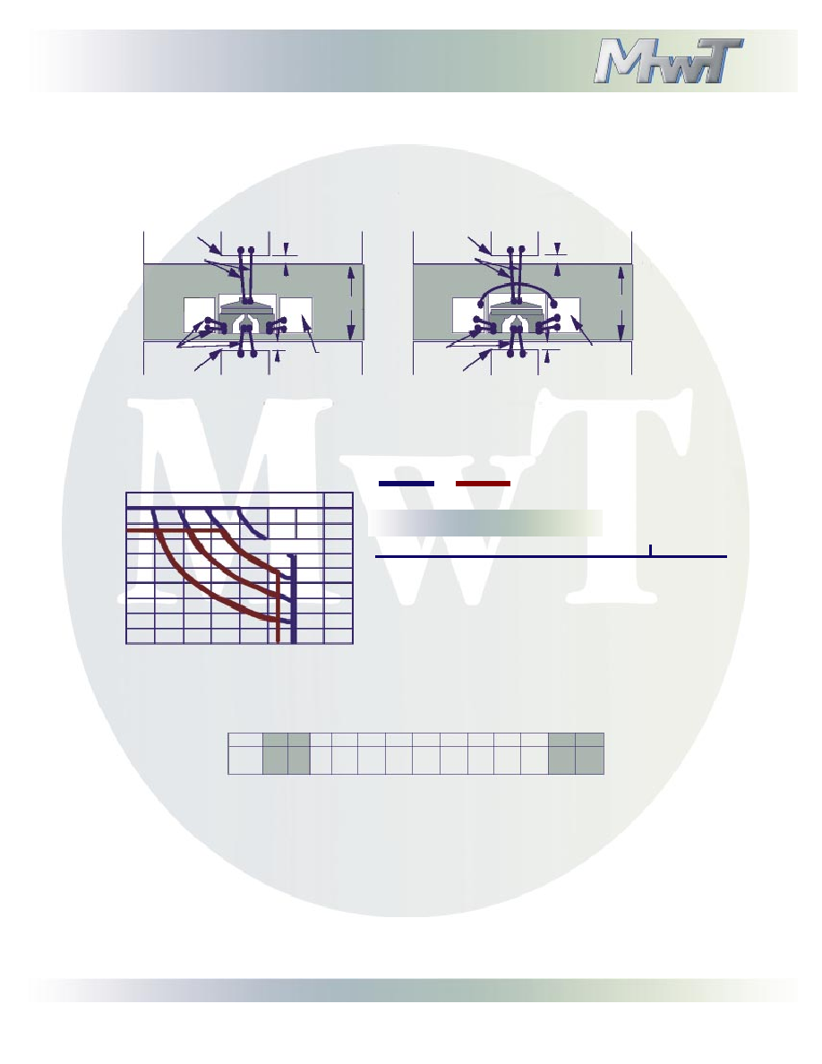
SAFE OPERATING LIMITS vs. BACKSIDE CHIP
MAXIMUM RATINGS AT Ta = 25
°°°°°C
SYMBOL
VDS
Tch
Tst
Pin
PARAMETER
UNITS
CONT MAX1
ABSOLUTE MAX2
Drain to Source Voltage
Channel Temperature
Storage Temperature
RF Input Power
See Safe Operating Limits
°°°°°C
200
+175
300
V
mW
-65 to +150
+150
NOTES: 1. Exceeding any one of these limits in continuous operation may reduce the
mean-time-to-failure below the design goals.
2. Exceeding any one of these limits may cause permanent damage.
MwT-9 And H9
DUAL BIAS
50
Output
Microstrip
50
Input
Microstrip
Output Reference
Plane
Input Reference
Plane
7 Mils Long
18 Mils Long
2 Mils
MwT
2 Mils
All Bond
Wires are 1.0
Mil Diameter
20 Mils
Copper Heat Sink
5 Mils Below Level of
Microstrip
Gold Ridge
10x 10x 5 Mils
(2 each)
FPH9
MwT-9 And H9
OPTIONAL BONDING
50
Output
Microstrip
50
Input
Microstrip
Output Reference
Plane
Input Reference
Plane
7 Mils Long
18 Mils Long
2 Mils
MwT
2 Mils
All Bond
Wires are 1.0
Mil Diameter
20 Mils
Copper Heat Sink
5 Mils Below Level of
Microstrip
Gold Ridge
10x 10x 5 For
Dual Bias, or
25pF Caps for
Single Bias
(2 each)
FPH9
MwT-H9
AlGaAs/InGaAs PHEMT
MAXIMUM RATINGS AT Ta = 25
°°°°°C
IDSS
(mA)
BIN#
1
2
3
126-
138
138-
150
150-
162
4
5
6
162-
174
174-
186
186-
198
78
9
198-
210
210-
222
222-
234
10
11
12
234-
246
246-
258
258-
270
13
270-
282
When placing order or inquiring, please specify BIN range, wafer no., if known, and screening level required.
BIN SELECTION
MwT-H9
AlGaAs/InGaAs PHEMT
BIN ACCURACY STATEMENT
相关PDF资料 |
PDF描述 |
|---|---|
| MWT-LP773 | KA BAND, GaAs, N-CHANNEL, RF SMALL SIGNAL, MESFET |
| MWT-LP7 | KA BAND, GaAs, N-CHANNEL, RF SMALL SIGNAL, MESFET |
| MWT-PH11 | X BAND, GaAs, N-CHANNEL, RF SMALL SIGNAL, HEMFET |
| MWT-PH15 | KA BAND, GaAs, N-CHANNEL, RF SMALL SIGNAL, MOSFET |
| MWT-PH16A | K BAND, GaAs, N-CHANNEL, RF POWER, HEMFET |
相关代理商/技术参数 |
参数描述 |
|---|---|
| MWTM 25/8]300/S | 制造商:Tyco Electronics 功能描述:Bulk |
| MWTM-10/3-1200-S(B25) | 制造商:TE Connectivity 功能描述:MWTM-10/3-1200-S(B25), |
| MWTM-16/5-A/U(B100) | 制造商:TE Connectivity 功能描述: |
| MWTZ100-10-C | 制造商:ITW Pancon 功能描述:MWTZ100-10-C / MAS-CON DOUBLE Z SPLICE - 100 SERIES |
| MWTZ100-12-C | 制造商:ITW Pancon 功能描述:MWTZ100-12-C / MAS-CON DOUBLE Z SPLICE - 100 SERIES |
发布紧急采购,3分钟左右您将得到回复。