- 您现在的位置:买卖IC网 > PDF目录9912 > MX7575KP+T (Maxim Integrated Products)IC ADC 8BIT MPU COMP 20-PLCC PDF资料下载
参数资料
| 型号: | MX7575KP+T |
| 厂商: | Maxim Integrated Products |
| 文件页数: | 8/12页 |
| 文件大小: | 0K |
| 描述: | IC ADC 8BIT MPU COMP 20-PLCC |
| 标准包装: | 1,000 |
| 位数: | 8 |
| 采样率(每秒): | 200k |
| 数据接口: | 并联 |
| 转换器数目: | 1 |
| 功率耗散(最大): | 15mW |
| 电压电源: | 单电源 |
| 工作温度: | 0°C ~ 70°C |
| 安装类型: | 表面贴装 |
| 封装/外壳: | 20-LCC(J 形引线) |
| 供应商设备封装: | 20-PLCC(9x9) |
| 包装: | 带卷 (TR) |
| 输入数目和类型: | 1 个单端,单极 |
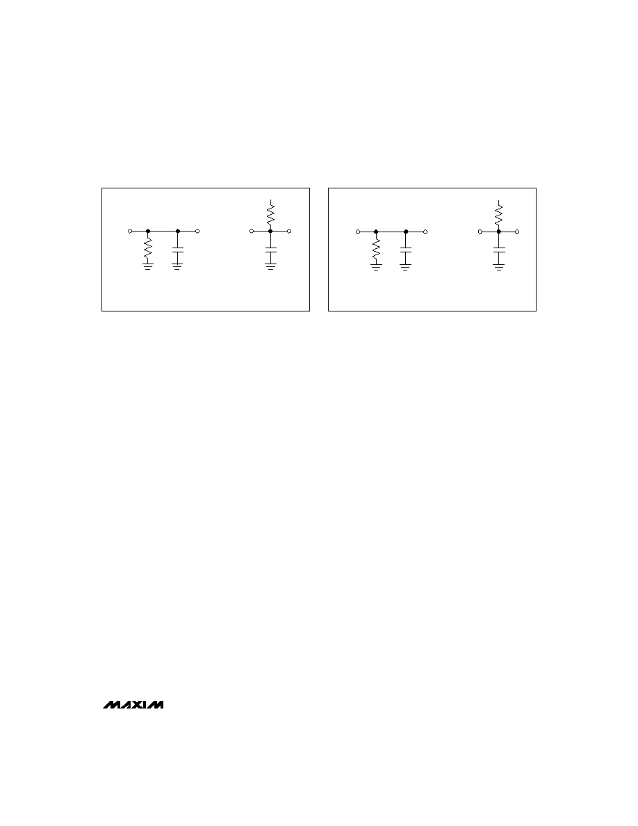
Figure 1. Load Circuits for Data-Access Time Test
_______________Detailed Description
Converter Operation
The MX7575 and MX7576 use the successive-approxi-
mation technique to convert an unknown analog input
voltage to an 8-bit digital output code (see
Functional
Diagrams). The MX7575 samples the input voltage on
an internal capacitor once (at the beginning of the con-
version), while the MX7576 samples the input signal
eight times during the conversion (see
MX7575
Track/Hold and MX7576 Analog Input sections). The
internal DAC is initially set to half scale, and the com-
parator determines whether the input signal is larger
than or smaller than half scale. If it is larger than half
scale, the DAC MSB is kept. But if it is smaller, the MSB
is dropped. At the end of each comparison phase, the
SAR (successive-approximation register) stores the
results of the previous decision and determines the
next trial bit. This information is then loaded into the
DAC after each decision. As the conversion proceeds,
the analog input is approximated more closely by com-
paring it to the combination of the previous DAC bits
and a new DAC trial bit. After eight comparison cycles,
the eight bits stored in the SAR are latched into the out-
put latches. At the end of the conversion, the
BUSY sig-
nal goes high, and the data in the output latches is
ready for microprocessor (P) access. Furthermore, the
DAC is reset to half scale in preparation for the next
conversion.
Microprocessor Interface
The
CS and RD logic inputs are used to initiate conver-
sions and to access data from the devices. The MX7575
and MX7576 have two common interface modes: slow-
memory interface mode and ROM interface mode. In
addition, the MX7576 has an asynchronous conversion
mode (MODE pin = low) where continuous conversions
are performed. In the slow-memory interface mode,
CS
and
RD are taken low to start a conversion and they
remain low until the conversion ends, at which time the
conversion result is latched. This mode is designed for
Ps that can be forced into a wait state. In the ROM
interface mode, however, the P is not forced into a wait
state. A conversion is started by taking
CS and RD low,
and data from the previous conversion is read. At the
end of the most recent conversion, the P executes a
read instruction and starts another conversion.
For the MX7575, TP should be hard-wired to VDD to
ensure proper operation of the device. Spurious signals
may occur on TP, or excessive currents may be drawn
from VDD if TP is left open or tied to a voltage other than
VDD.
Slow-Memory Mode
Figure 3 shows the timing diagram for slow-memory
interface mode. This is used with Ps that have a wait-
state capability of at least 10s (such as the 8085A),
where a read instruction is extended to accommodate
slow-memory devices. A conversion is started by exe-
cuting a memory read to the device (taking
CS and RD
low). The
BUSY signal (which is connected to the P
READY input) then goes low and forces the P into a
wait state. The MX7575 track/hold, which had been
tracking the analog input signal, holds the signal on the
third falling clock edge after
RD goes low (Figure 12).
The MX7576, however, samples the analog input eight
times during a conversion (once before each compara-
tor decision). At the end of the conversion,
BUSY
returns high, the output latches and buffers are updat-
ed with the new conversion result, and the P com-
pletes the memory read by acquiring this new data.
The fast conversion time of the MX7575/MX7576
ensures that the P is not forced into a wait state for an
excessive amount of time. Faster versions of many Ps,
MX7575/MX7576
CMOS, P-Compatible, 5s/10s, 8-Bit ADCs
_______________________________________________________________________________________
5
D_
100pF
DGND
+5V
100pF
3k
a) HIGH-Z TO VOH
NOTE: D_ REPRESENTS ANY OF THE DATA OUTPUTS
b) HIGH-Z TO VOL
D_
10pF
DGND
+5V
10pF
3k
a) VOH TO HIGH-Z
b) VOL TO HIGH-Z
NOTE: D_ REPRESENTS ANY OF THE DATA OUTPUTS
Figure 2. Load Circuits for Data-Hold Time Test
相关PDF资料 |
PDF描述 |
|---|---|
| MS3120E16-26P | CONN RCPT 26POS WALL MNT W/PINS |
| MAX1246BCEE+T | IC ADC 12BIT SERIAL 16-QSOP |
| MS27468E23F53P | CONN RCPT 53POS JAM NUT W/PINS |
| IDT72V291L10TFG | IC FIFO SS 32768X36 10NS 64QFP |
| MAX1240CCPA+ | IC ADC 12BIT SERIAL 8-DIP |
相关代理商/技术参数 |
参数描述 |
|---|---|
| MX7575SQ | 功能描述:模数转换器 - ADC 8-Bit Precision DAC RoHS:否 制造商:Texas Instruments 通道数量:2 结构:Sigma-Delta 转换速率:125 SPs to 8 KSPs 分辨率:24 bit 输入类型:Differential 信噪比:107 dB 接口类型:SPI 工作电源电压:1.7 V to 3.6 V, 2.7 V to 5.25 V 最大工作温度:+ 85 C 安装风格:SMD/SMT 封装 / 箱体:VQFN-32 |
| MX7575SQ/883B | 功能描述:模数转换器 - ADC 8-Bit Precision DAC RoHS:否 制造商:Texas Instruments 通道数量:2 结构:Sigma-Delta 转换速率:125 SPs to 8 KSPs 分辨率:24 bit 输入类型:Differential 信噪比:107 dB 接口类型:SPI 工作电源电压:1.7 V to 3.6 V, 2.7 V to 5.25 V 最大工作温度:+ 85 C 安装风格:SMD/SMT 封装 / 箱体:VQFN-32 |
| MX7575TQ | 功能描述:模数转换器 - ADC 8-Bit Precision DAC RoHS:否 制造商:Texas Instruments 通道数量:2 结构:Sigma-Delta 转换速率:125 SPs to 8 KSPs 分辨率:24 bit 输入类型:Differential 信噪比:107 dB 接口类型:SPI 工作电源电压:1.7 V to 3.6 V, 2.7 V to 5.25 V 最大工作温度:+ 85 C 安装风格:SMD/SMT 封装 / 箱体:VQFN-32 |
| MX7575TQ/883B | 功能描述:模数转换器 - ADC 8-Bit Precision DAC RoHS:否 制造商:Texas Instruments 通道数量:2 结构:Sigma-Delta 转换速率:125 SPs to 8 KSPs 分辨率:24 bit 输入类型:Differential 信噪比:107 dB 接口类型:SPI 工作电源电压:1.7 V to 3.6 V, 2.7 V to 5.25 V 最大工作温度:+ 85 C 安装风格:SMD/SMT 封装 / 箱体:VQFN-32 |
| MX7576 | 制造商:未知厂家 制造商全称:未知厂家 功能描述:CMOS.µ.P Compatible.5µ.s/10µ.s.8-Bit ADCs |
发布紧急采购,3分钟左右您将得到回复。