- 您现在的位置:买卖IC网 > PDF目录2038 > N74F574D,602 (NXP Semiconductors)IC FLIP FLOP TRI-ST OCTAL 20SOIC PDF资料下载
参数资料
| 型号: | N74F574D,602 |
| 厂商: | NXP Semiconductors |
| 文件页数: | 7/14页 |
| 文件大小: | 0K |
| 描述: | IC FLIP FLOP TRI-ST OCTAL 20SOIC |
| 产品培训模块: | Logic Packages |
| 标准包装: | 1,520 |
| 系列: | 74F |
| 功能: | 标准 |
| 类型: | D 型总线 |
| 输出类型: | 三态非反相 |
| 元件数: | 1 |
| 每个元件的位元数: | 8 |
| 频率 - 时钟: | 100MHz |
| 延迟时间 - 传输: | 3.2ns |
| 触发器类型: | 正边沿 |
| 输出电流高,低: | 3mA,24mA |
| 电源电压: | 4.5 V ~ 5.5 V |
| 工作温度: | 0°C ~ 70°C |
| 安装类型: | 表面贴装 |
| 封装/外壳: | 20-SOIC(0.295",7.50mm 宽) |
| 包装: | 管件 |
Philips Semiconductors
Product specification
74F573/74F574
Latch/flip-flop
74F573 Octal Transparent Latch (3-State)
74F574 Octal D Flip-Flop (3-State)
2
1989 Oct 16
853-0083 97897
FEATURES
74F573 is broadside pinout version of 74F373
74F574 is broadside pinout version of 74F374
Inputs and Outputs on opposite side of package allow easy
interface to Microprocessors
Useful as an Input or Output port for Microprocessors
3-State Outputs for Bus interfacing
Common Output Enable
74F563 and 74F564 are inverting version of 74F573 and 74F574
respectively
3-State Outputs glitch free during power-up and power-down
These are High-Speed replacements for N8TS805 and N8TS806
DESCRIPTION
The 74F573 is an octal transparent latch coupled to eight 3-State
output buffers. The two sections of the device are controlled
independently by Enable (E) and Output Enable (OE) control gates.
The 74F573 is functionally identical to the 74F373 but has a
broadside pinout configuration to facilitate PC board layout and
allow easy interface with microprocessors.
The data on the D inputs is transferred to the latch outputs when the
Enable (E) input is High. The latch remains transparent to the data
input while E is High and stores the data that is present one setup
time before the High-to-Low enable transition.
The 3-State output buffers are designed to drive heavily loaded
3-State buses, MOS memories, or MOS microprocessors. The
active Low Output Enable (OE) controls all eight 3-State buffers
independent to the latch operation. When OE is Low, the latched or
transparent data appears at the outputs. When OE is High, the
outputs are in high impedance “off” state, which means they will
neither drive nor load the bus.
The 74F574 is functionally identical to the 74F374 but has a
broadside pinout configuration to facilitate PC board layout and
allow easy interface with microprocesors.
It is an 8-bit, edge triggered register coupled to eight 3-State output
buffers. The two sections of the device are controlled independently
by the clock (CP) and Output Enable (OE) control gates.
The register is fully edge-triggered. The state of each D input, one
setup time before the Low-to-High clock transition is transferred to
the corresponding flip-flop’s Q output.
The 3-State output buffers are designed to drive heavily loaded
3-State buses, MOS memories, or MOS microprocessors. The
active Low Output Enable (OE) controls all eight 3-State buffers
independently of the latch operation. When OE is Low, the latched
or transparent data appears at the outputs. When OE is High, the
outputs are in high impedance “off” state, which means they will
neither drive nor load the bus.
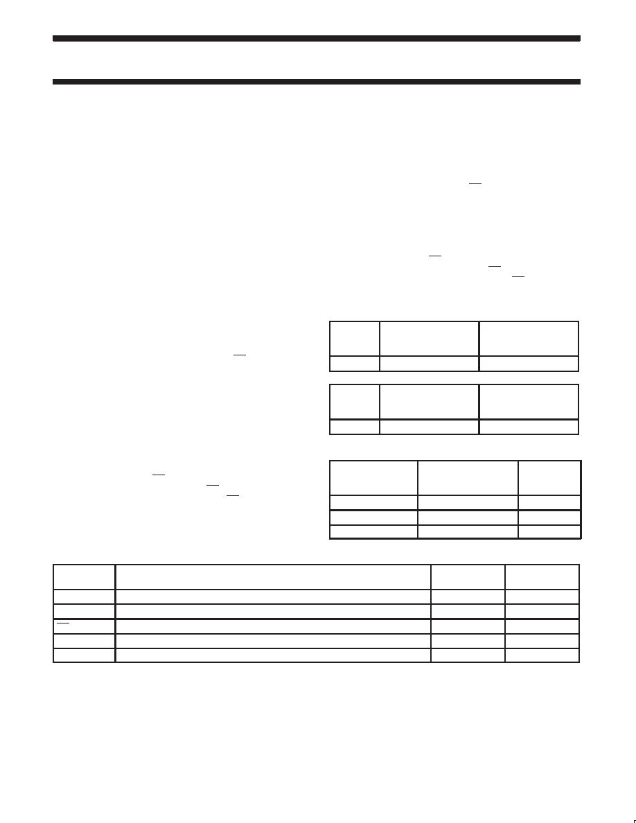
TYPE
TYPICAL
PROPAGATION DELAY
TYPICAL SUPPLY
CURRENT
(TOTAL)
74F573
5.0ns
35mA
TYPE
TYPICAL fMAX
TYPICAL SUPPLY
CURRENT
(TOTAL)
74F574
180MHz
50mA
ORDERING INFORMATION
DESCRIPTION
COMMERCIAL RANGE
VCC = 5V ±10%,
Tamb = 0°C to +70°C
PKG DWG #
20-Pin Plastic DIP
N74F573N, N74F574N
SOT146-1
20-Pin Plastic SOL
N74F573D, N74F574D
SOT163-1
20-Pin Plastic SSOP
N74F573DB
SOT339-1
INPUT AND OUTPUT LOADING AND FAN-OUT TABLE
PINS
DESCRIPTION
74F (U.L.)
HIGH/LOW
LOAD VALUE
HIGH/LOW
D0 - D7
Data inputs
1.0/1.0
20
A/0.6mA
E (74F573)
Latch Enable input (active falling edge)
1.0/1.0
20
A/0.6mA
OE
Output Enable input (active Low)
1.0/1.0
20
A/0.6mA
CP (74F574)
Clock Pulse input (active rising edge)
1.0/1.0
20
A/0.6mA
Q0 - Q7
3-State outputs
150/40
3.0mA/24mA
NOTE: One (1.0) FAST Unit Load is defined as: 20
A in the High state and 0.6mA in the Low state.
相关PDF资料 |
PDF描述 |
|---|---|
| N74F579N,602 | IC COUNTER 8BIT BINARY 20DIP |
| N74F640D,623 | IC TRANSCVR 3ST 8BIT INV 20SOIC |
| N74F827DB,112 | IC BUFF DVR TRI-ST 10BIT 24SSOP |
| NB4L52MNR2G | IC FLIP FLOP DATA/CLK DFF 16-QFN |
| NB7V52MMNHTBG | IC FLIP FLOP DATA/CLOCK D 16-QFN |
相关代理商/技术参数 |
参数描述 |
|---|---|
| N74F574DB | 制造商:未知厂家 制造商全称:未知厂家 功能描述:Octal D-Type Flip-Flop |
| N74F574D-T | 制造商:未知厂家 制造商全称:未知厂家 功能描述:Octal D-Type Flip-Flop |
| N74F574N | 功能描述:触发器 OCTAL D FLIP-FLOP RoHS:否 制造商:Texas Instruments 电路数量:2 逻辑系列:SN74 逻辑类型:D-Type Flip-Flop 极性:Inverting, Non-Inverting 输入类型:CMOS 输出类型: 传播延迟时间:4.4 ns 高电平输出电流:- 16 mA 低电平输出电流:16 mA 电源电压-最大:5.5 V 最大工作温度:+ 85 C 安装风格:SMD/SMT 封装 / 箱体:X2SON-8 封装:Reel |
| N74F574N,602 | 功能描述:触发器 OCTAL D FLIP-FLOP RoHS:否 制造商:Texas Instruments 电路数量:2 逻辑系列:SN74 逻辑类型:D-Type Flip-Flop 极性:Inverting, Non-Inverting 输入类型:CMOS 输出类型: 传播延迟时间:4.4 ns 高电平输出电流:- 16 mA 低电平输出电流:16 mA 电源电压-最大:5.5 V 最大工作温度:+ 85 C 安装风格:SMD/SMT 封装 / 箱体:X2SON-8 封装:Reel |
| N74F574N-B | 制造商:未知厂家 制造商全称:未知厂家 功能描述:Octal D-Type Flip-Flop |
发布紧急采购,3分钟左右您将得到回复。