- 您现在的位置:买卖IC网 > PDF目录189003 > NAND08GW4B3BN6T (STMICROELECTRONICS) 512M X 16 FLASH 3V PROM, 35 ns, PDSO48 PDF资料下载
参数资料
| 型号: | NAND08GW4B3BN6T |
| 厂商: | STMICROELECTRONICS |
| 元件分类: | PROM |
| 英文描述: | 512M X 16 FLASH 3V PROM, 35 ns, PDSO48 |
| 封装: | 12 X 20 MM, PLASTIC, TSOP-48 |
| 文件页数: | 28/59页 |
| 文件大小: | 998K |
| 代理商: | NAND08GW4B3BN6T |
第1页第2页第3页第4页第5页第6页第7页第8页第9页第10页第11页第12页第13页第14页第15页第16页第17页第18页第19页第20页第21页第22页第23页第24页第25页第26页第27页当前第28页第29页第30页第31页第32页第33页第34页第35页第36页第37页第38页第39页第40页第41页第42页第43页第44页第45页第46页第47页第48页第49页第50页第51页第52页第53页第54页第55页第56页第57页第58页第59页
NAND512-B, NAND01G-B, NAND02G-B, NAND04G-B, NAND08G-B
34/59
Blocks Lock-Down
The Lock-Down feature provides an additional lev-
el of protection. A Locked-down block cannot be
unlocked by a software command. Locked-Down
blocks can only be unlocked by setting the Write
Protect signal to Low for a minimum of 100ns.
Only locked blocks can be locked-down. The com-
mand has no affect on unlocked blocks.
Refer to Figure 25., Command Latch AC Wave-
forms for details on how to issue the command.
Block Lock Status
In Block Lock mode (PRL High) the Block Lock
Status of each block can be checked by issuing a
Read Block Lock Status command (see Table
The command consists of:
■
one bus cycle to give the command code
■
three bus cysles to give the block address
After this, a read cycle will then output the Block
Lock Status on the I/O pins on the falling edge of
Chip Enable or Read Enable, whichever occurs
last. Chip Enable or Read Enable do not need to
be toggled to update the status.
The Read Block Lock Status command will not be
accepted while the device is busy (RB Low).
The device will remain in Read Block Lock Status
mode until another command is issued.
If the device is not in the Block Lock mode (PRL
Low) the Block Status can be read in the Status
Register using the Read Status Register com-
mand.
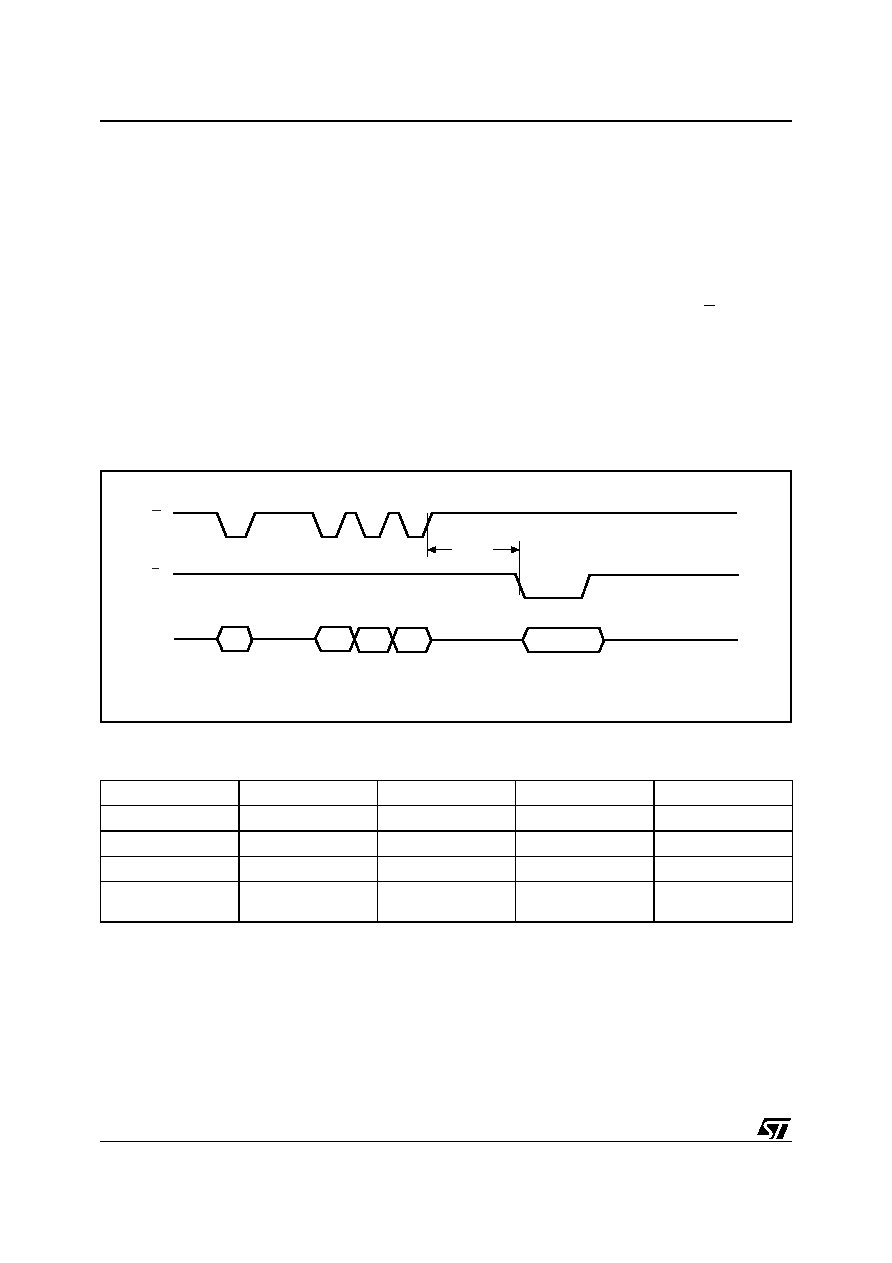
Figure 20. Read Block Lock Status Operation
Note: Three address cycles are required for 2,4 and 8 Gb devices. The 512Mb and 1Gb devices only require two address cycles.
Table 16. Block Lock Status
Note: X = Don’t Care.
Status
I/O7-I/O3
I/O2
I/O1
I/O0
Locked
X
0
1
0
Unlocked
X
1
0
Locked-Down
X
0
1
Unlocked in Locked-
Down Area
X1
0
1
I/O
R
Block Address, 3 cycles
ai08669
7Ah
Read Block Lock
Status Command
Add1
Add2
Add3
Dout
Block Lock Status
tWHRL
W
相关PDF资料 |
PDF描述 |
|---|---|
| NAND08GR3B2AN1F | 1G X 8 FLASH 1.8V PROM, 35 ns, PDSO48 |
| NAND04GW4B2AN1E | 256M X 16 FLASH 3V PROM, 35 ns, PDSO48 |
| NAND02GW4B2AN1T | 128M X 16 FLASH 3V PROM, 35 ns, PDSO48 |
| NAND04GR4B2CN1F | 256M X 16 FLASH 1.8V PROM, 35 ns, PDSO48 |
| NAND08GW3B2CZL1F | 1G X 8 FLASH 3V PROM, 25000 ns, PBGA52 |
相关代理商/技术参数 |
参数描述 |
|---|---|
| NAND128W3A0AN6 | 功能描述:闪存 NAND & S.MEDIA FLASH RoHS:否 制造商:ON Semiconductor 数据总线宽度:1 bit 存储类型:Flash 存储容量:2 MB 结构:256 K x 8 定时类型: 接口类型:SPI 访问时间: 电源电压-最大:3.6 V 电源电压-最小:2.3 V 最大工作电流:15 mA 工作温度:- 40 C to + 85 C 安装风格:SMD/SMT 封装 / 箱体: 封装:Reel |
| NAND128W3A0AN6E | 功能描述:闪存 2.7-3.6V 128M(16Mx8) RoHS:否 制造商:ON Semiconductor 数据总线宽度:1 bit 存储类型:Flash 存储容量:2 MB 结构:256 K x 8 定时类型: 接口类型:SPI 访问时间: 电源电压-最大:3.6 V 电源电压-最小:2.3 V 最大工作电流:15 mA 工作温度:- 40 C to + 85 C 安装风格:SMD/SMT 封装 / 箱体: 封装:Reel |
| NAND128W3A0AN6F | 功能描述:闪存 NAND & S.MEDIA FLASH RoHS:否 制造商:ON Semiconductor 数据总线宽度:1 bit 存储类型:Flash 存储容量:2 MB 结构:256 K x 8 定时类型: 接口类型:SPI 访问时间: 电源电压-最大:3.6 V 电源电压-最小:2.3 V 最大工作电流:15 mA 工作温度:- 40 C to + 85 C 安装风格:SMD/SMT 封装 / 箱体: 封装:Reel |
| NAND128W3A0BN6E | 功能描述:闪存 2.7-3.6V 128M(16Mx8) RoHS:否 制造商:ON Semiconductor 数据总线宽度:1 bit 存储类型:Flash 存储容量:2 MB 结构:256 K x 8 定时类型: 接口类型:SPI 访问时间: 电源电压-最大:3.6 V 电源电压-最小:2.3 V 最大工作电流:15 mA 工作温度:- 40 C to + 85 C 安装风格:SMD/SMT 封装 / 箱体: 封装:Reel |
| NAND128W3A0BN6F | 功能描述:闪存 NAND & S.MEDIA FLASH RoHS:否 制造商:ON Semiconductor 数据总线宽度:1 bit 存储类型:Flash 存储容量:2 MB 结构:256 K x 8 定时类型: 接口类型:SPI 访问时间: 电源电压-最大:3.6 V 电源电压-最小:2.3 V 最大工作电流:15 mA 工作温度:- 40 C to + 85 C 安装风格:SMD/SMT 封装 / 箱体: 封装:Reel |
发布紧急采购,3分钟左右您将得到回复。