- 您现在的位置:买卖IC网 > PDF目录8645 > NB100EP223FAR2 (ON Semiconductor)IC CLOCK BUFFER MUX 2:22 64-LQFP PDF资料下载
参数资料
| 型号: | NB100EP223FAR2 |
| 厂商: | ON Semiconductor |
| 文件页数: | 6/10页 |
| 文件大小: | 0K |
| 描述: | IC CLOCK BUFFER MUX 2:22 64-LQFP |
| 产品变化通告: | Product Obsolescence 01/Jul/2005 |
| 标准包装: | 1 |
| 系列: | 100EP |
| 类型: | 扇出缓冲器(分配),多路复用器 |
| 电路数: | 1 |
| 比率 - 输入:输出: | 2:22 |
| 差分 - 输入:输出: | 是/是 |
| 输入: | HSTL,LVDS,LVPECL |
| 输出: | HSTL |
| 频率 - 最大: | 500MHz |
| 电源电压: | 3 V ~ 3.6 V |
| 工作温度: | 0°C ~ 85°C |
| 安装类型: | 表面贴装 |
| 封装/外壳: | 64-LQFP 裸露焊盘 |
| 供应商设备封装: | 64-LQFP(10x10) |
| 包装: | 剪切带 (CT) |
| 其它名称: | NB100EP223FAROSCT |
NB100EP223
http://onsemi.com
5
Symbol
Characteristic
0°C
25°C
85°C
Unit
Min
Typ
Max
Min
Typ
Max
Min
Typ
Max
VOpp
Differential Output Voltage
(Figure 3)
fout < 500 MHz
600
750
600
750
600
700
mV
tPLH
tPHL
Propagation Delay (Differential)
LVPECL_CLK to Q
HSTL_CLK to Q
700
800
900
1000
1100
750
850
900
950
1100
1200
800
850
1000
1050
1300
1350
ps
tskew
WithinDevice Skew (Note 5)
DevicetoDevice Skew (Note 6)
25
100
50
250
30
200
65
450
50
250
115
450
ps
tJITTER
Random Clock Jitter (Figure 3) (RMS)
0.5
2
0.5
2
0.5
2
ps
VPP
Input Swing (Differential Mode)
LVPECL, HSTL
150
800
1200
150
800
1200
150
800
1200
mV
tS
OE Set Up Time (Note 7)
1.0
ns
tH
OE Hold Time
0.5
ns
tr/tf
Output Rise/Fall Time (20%80%)
300
450
700
275
450
700
350
500
750
ps
NOTE: Device will meet the specifications after thermal equilibrium has been established when mounted in a test socket or printed circuit
board with maintained transverse airflow greater than 500 lfpm. Electrical parameters are guaranteed only over the declared
operating temperature range. Functional operation of the device exceeding these conditions is not implied. Device specification limit
values are applied individually under normal operating conditions and not valid simultaneously.
4. Measured with 750 mV (LVPECL) source or 1 V (HSTL) source, 50% duty cycle clock source. All outputs loaded with 50 W to ground
(See Figure 6).
5. Skew is measured between outputs under identical transitions and conditions on any one device.
6. DevicetoDevice skew for identical transitions at identical VCC levels.
7. OE Set Up Time is defined with respect to the rising edge of the clock. OE HightoLow transition ensures outputs remain disabled during
the next clock cycle. OE LowtoHigh transition enables normal operation of the next input clock (See Figure 7).
8. VPP is the differential input voltage swing required to maintain AC characteristics including tPD and devicetodevice skew.
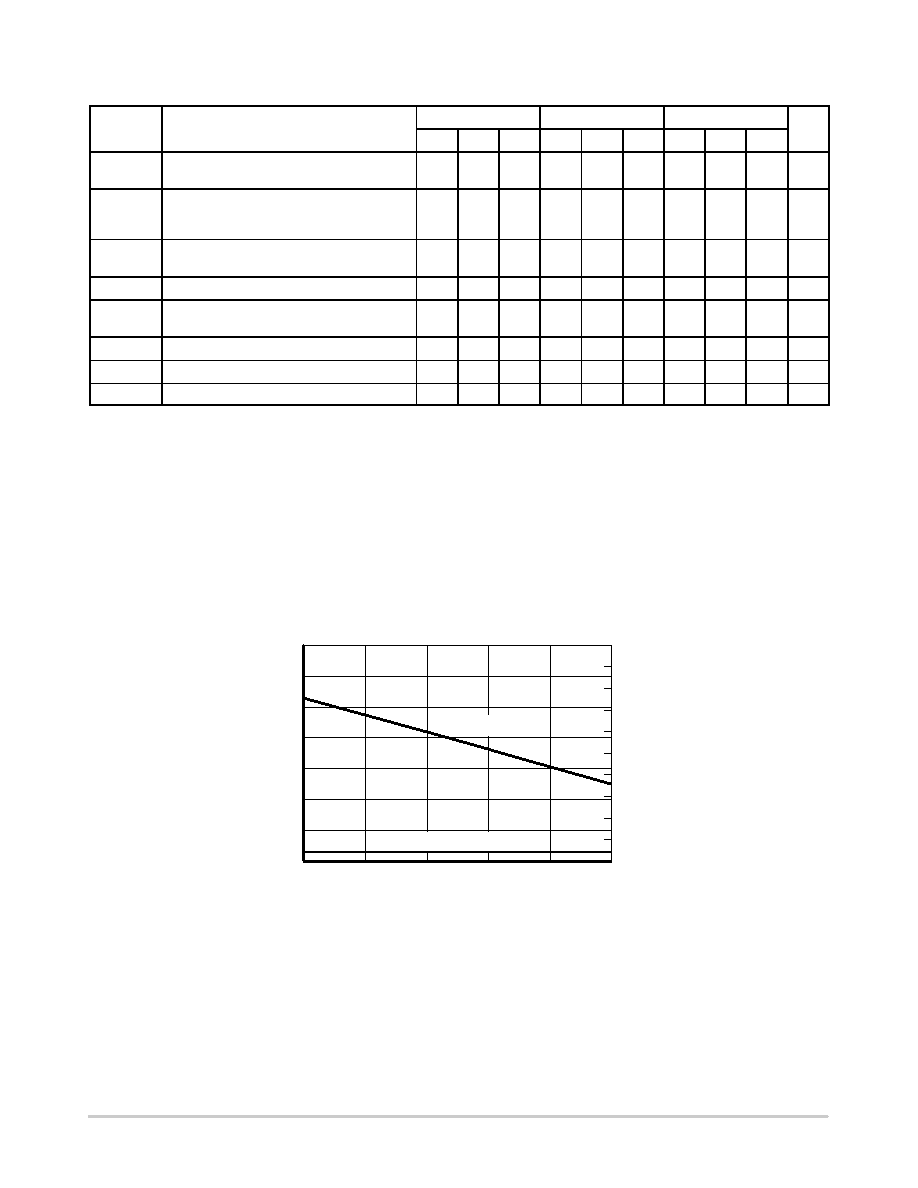
Figure 3. Output Frequency (FOUT) versus Output Voltage (VOPP) and Random Clock Jitter (tJITTER)
FREQUENCY (GHz)
0.5
0.6
0.7
0.8
0.9
1.0
800
900
700
600
500
400
300
200
OUTPUT
AMPLITUDE
(mV)
9.0
8.0
7.0
6.0
5.0
4.0
3.0
2.0
1.0
0
10
RMS
JITTER
(ps)
Q AMP (mV)
RMS JITTER (ps)
相关PDF资料 |
PDF描述 |
|---|---|
| AD7225BRSZ | IC DAC 8BIT QUAD W/AMP 24SSOP |
| VI-21M-IV-F1 | CONVERTER MOD DC/DC 10V 150W |
| LTC2641CDD-14#PBF | IC DAC 14BIT VOUT 8-DFN |
| VI-21M-IV-F4 | CONVERTER MOD DC/DC 10V 150W |
| DAC8228FPZ | IC DAC 8BIT DUAL V-OUT 20DIP |
相关代理商/技术参数 |
参数描述 |
|---|---|
| NB100EP223FAR2G | 功能描述:时钟驱动器及分配 3.3V 1:22 HSTL/PECL to HSLT Clock Driver RoHS:否 制造商:Micrel 乘法/除法因子:1:4 输出类型:Differential 最大输出频率:4.2 GHz 电源电压-最大: 电源电压-最小:5 V 最大工作温度:+ 85 C 封装 / 箱体:SOIC-8 封装:Reel |
| NB100LVEP17 | 制造商:ONSEMI 制造商全称:ON Semiconductor 功能描述:2.5V / 3.3V Quad Differential Driver/Receiver |
| NB100LVEP17/D | 制造商:未知厂家 制造商全称:未知厂家 功能描述:2.5V / 3.3V ECL Quad Differential Driver/Receiver |
| NB100LVEP17DT | 功能描述:总线接收器 2.5V/3.3V/5V ECL RoHS:否 制造商:Texas Instruments 接收机数量:4 接收机信号类型:Differential 接口类型:EIA/TIA-422-B, V.11 工作电源电压:3.3 V 最大工作温度:+ 85 C 最小工作温度:- 40 C 封装 / 箱体:TSSOP-16 封装:Reel |
| NB100LVEP17DTG | 功能描述:总线接收器 2.5V/3.3V/5V ECL Quad Diff Driver RoHS:否 制造商:Texas Instruments 接收机数量:4 接收机信号类型:Differential 接口类型:EIA/TIA-422-B, V.11 工作电源电压:3.3 V 最大工作温度:+ 85 C 最小工作温度:- 40 C 封装 / 箱体:TSSOP-16 封装:Reel |
发布紧急采购,3分钟左右您将得到回复。