- 您现在的位置:买卖IC网 > PDF目录9752 > NB100LVEP17MNG (ON Semiconductor)IC DRVR ECL QUAD 2.5V/3.3V 24QFN PDF资料下载
参数资料
| 型号: | NB100LVEP17MNG |
| 厂商: | ON Semiconductor |
| 文件页数: | 7/10页 |
| 文件大小: | 0K |
| 描述: | IC DRVR ECL QUAD 2.5V/3.3V 24QFN |
| 标准包装: | 92 |
| 系列: | 100LVEP |
| 逻辑类型: | 差分接收器/驱动器 |
| 电源电压: | 2.375 V ~ 3.8 V |
| 位数: | 4 |
| 工作温度: | -40°C ~ 85°C |
| 安装类型: | 表面贴装 |
| 封装/外壳: | 24-VFQFN 裸露焊盘 |
| 供应商设备封装: | 24-QFN(4x4) |
| 包装: | 管件 |
| 其它名称: | NB100LVEP17MNGOS |
NB100LVEP17
http://onsemi.com
6
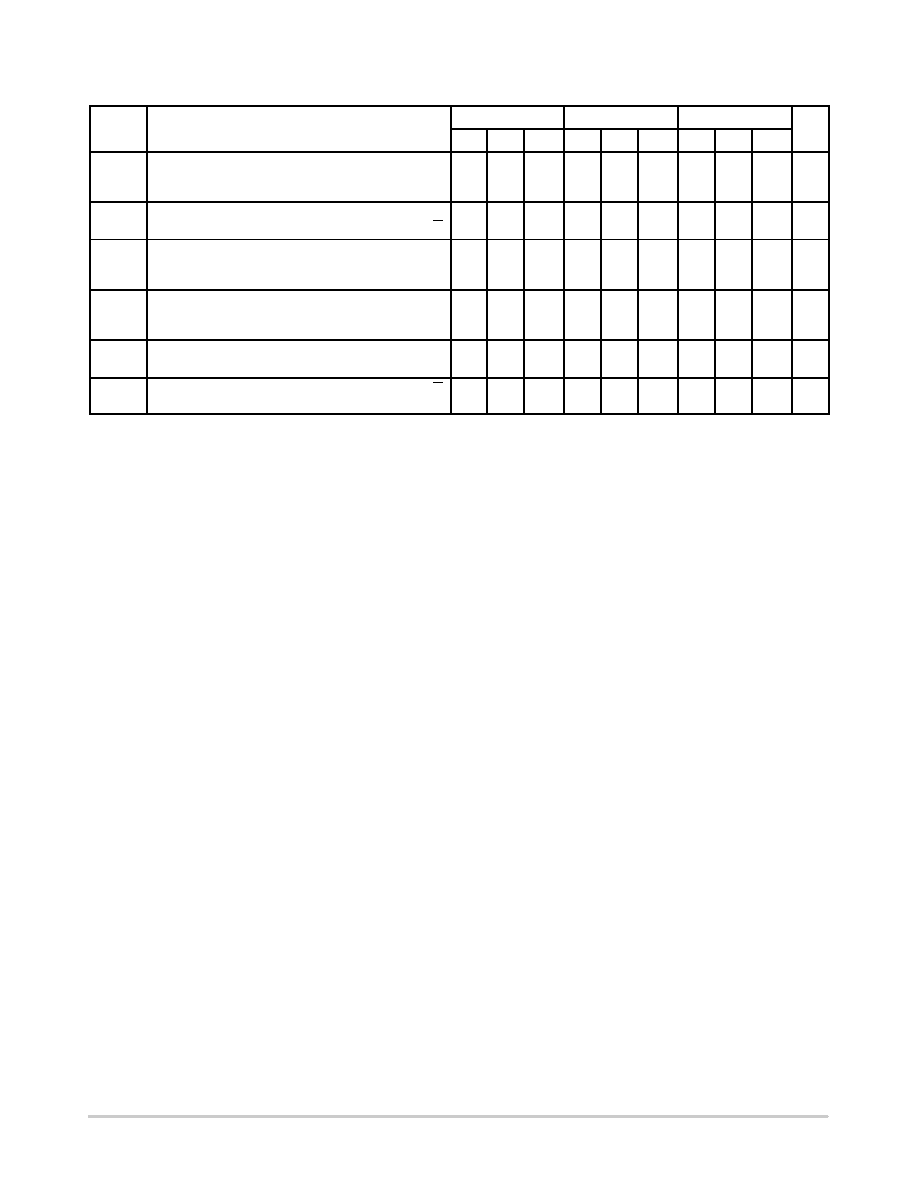
Table 7. AC CHARACTERISTICS VCC = 0 V; VEE = 2.375 V to 3.8 V or VCC = 2.375 V to 3.8 V; VEE = 0 V (Note 14)
Symbol
Characteristic
40°C
25°C
85°C
Unit
Min
Typ
Max
Min
Typ
Max
Min
Typ
Max
VOUTPP Output Voltage Amplitude
fin < 1 GHz
(See Figures 4, 5)
fin = 2 GHz
fin = 2.5 GHz
600
400
300
700
500
400
600
325
250
700
500
400
550
300
200
700
500
400
mV
tPLH,
tPHL
Propagation Delay to Output Differential
D to Q, Q
200
250
325
200
250
325
225
300
350
ps
tSkew
Pulse Skew (Note 15)
Within Device Skew (Note 17)
DevicetoDevice Skew (Note 17)
5
25
100
5
25
100
5
25
100
ps
tJITTER
RMS Random Clock Jitter (Note 18)
fin = 2.5 GHz
Peakto Peak Data Dependent Jitter
fin = 1.5 Gb/s
(Note 19)
fin = 2.5 Gb/s
0.5
5
1
15
0.5
5
1
15
0.5
5
1
15
ps
VINPP
Input Voltage Swing (Differential Configuration)
(Note 20)
150
800
1200
150
800
1200
150
800
1200
mV
tr
tf
Output Rise/Fall Times @ 50 MHz
Q, Q
(20% 80%)
125
175
225
140
190
240
150
200
250
ps
NOTE: Device will meet the specifications after thermal equilibrium has been established when mounted in a test socket or printed circuit
board with maintained transverse airflow greater than 500 lfpm. Electrical parameters are guaranteed only over the declared
operating temperature range. Functional operation of the device exceeding these conditions is not implied. Device specification limit
values are applied individually under normal operating conditions and not valid simultaneously.
14.Measured using a 750 mV source, 50% duty cycle clock source. All loading with 50 W to VCC 2.0 V. Input edge rates 150 ps (20% 80%).
15.Pulse Skew = |tPLH tPHL|
16.Worst case difference between Q0 and Q1 outputs.
17.Skew is measured between outputs under identical transitions.
18.Additive RMS jitter with 50% Duty Cycle Clock Signal at 2.5 GHz.
19.PeaktoPeak jitter with input NRZ data at PRBS 2311 at 2.5 Gb/s with all inputs active.
20.Input voltage swing is a singleended measurement operating in differential mode, with minimum propagation change of 50 ps.
相关PDF资料 |
PDF描述 |
|---|---|
| VI-25D-IU-F4 | CONVERTER MOD DC/DC 85V 200W |
| MC10EP17DTG | IC RCVR/DRVR QUAD ECL DF 20TSSOP |
| MAX1229ACEP+ | IC ADC 12BIT 300KSPS 20-QSOP |
| M83723/83R12038 | CONN RCPT 3POS WALL MT W/PINS |
| DS26518GNB1+ | IC TXRX T1/E1/J1 8PRT 256-CSBGA |
相关代理商/技术参数 |
参数描述 |
|---|---|
| NB100LVEP17MNR2 | 功能描述:总线接收器 2.5V/3.3V/5V ECL RoHS:否 制造商:Texas Instruments 接收机数量:4 接收机信号类型:Differential 接口类型:EIA/TIA-422-B, V.11 工作电源电压:3.3 V 最大工作温度:+ 85 C 最小工作温度:- 40 C 封装 / 箱体:TSSOP-16 封装:Reel |
| NB100LVEP17MNR2G | 功能描述:总线接收器 2.5V/3.3V/5V ECL Quad Diff Driver RoHS:否 制造商:Texas Instruments 接收机数量:4 接收机信号类型:Differential 接口类型:EIA/TIA-422-B, V.11 工作电源电压:3.3 V 最大工作温度:+ 85 C 最小工作温度:- 40 C 封装 / 箱体:TSSOP-16 封装:Reel |
| NB100LVEP1MNG | 制造商:ON Semiconductor 功能描述: |
| NB100LVEP221 | 制造商:ONSEMI 制造商全称:ON Semiconductor 功能描述:2.5V/3.3V 1:20 Differential HSTL/ECL/PECL Clock Driver |
| NB100LVEP221/D | 制造商:ONSEMI 制造商全称:ON Semiconductor 功能描述:2.5V/3.3V 1:20 Differential HSTL/ECL/PECL Clock Driver |
发布紧急采购,3分钟左右您将得到回复。