参数资料
| 型号: | NB3N3010BDR2G |
| 厂商: | ON Semiconductor |
| 文件页数: | 5/9页 |
| 文件大小: | 0K |
| 描述: | IC CLOCK GENERATOR PLL 8SOIC |
| 标准包装: | 2,500 |
| 类型: | 时钟/频率发生器 |
| PLL: | 无 |
| 主要目的: | USB 应用 |
| 输入: | 时钟 |
| 输出: | LVCMOS |
| 电路数: | 1 |
| 比率 - 输入:输出: | 1:2 |
| 差分 - 输入:输出: | 无/无 |
| 频率 - 最大: | 12.288MHz |
| 电源电压: | 3.135 V ~ 3.465 V |
| 工作温度: | 0°C ~ 85°C |
| 安装类型: | 表面贴装 |
| 封装/外壳: | 8-SOIC(0.154",3.90mm 宽) |
| 供应商设备封装: | 8-SOICN |
| 包装: | 带卷 (TR) |
NB3N3010B
http://onsemi.com
5
APPLICATION INFORMATION
Figure 1 shows the simplified block diagram of the
NB3N3010B device.
The primary function of the NB3N3010B is to accept a
selectable 4 kHz or 8 kHz input reference clock, REF, and
then multiply it to 12.288 MHz output frequency.
Frequency Select SO
Either of two expected input REF frequencies, 4 kHz or
8 kHz, will be multiplied by the FLL to achieve 12.288 MHz
at the lowskew CLKA and CLKB outputs by selecting the
S0 pin; see Table 6.
The pulse high time (THI) of the input reference signal may
vary widely depending on the application. See AC
specifications for details.
Output Enable ENABLEn
A Low active output enable input pin, ENABLEn, is
provided. When the ENABLEn input is High inactive, both
clock outputs are driven to a logic Low.
The NB3N3010B implements a delay, specified as
ENABLEn to Output Delay in the AC Specifications, from
the assertion of ENABLEn to the first rising edges on the
clock outputs. This delay insures that CLKA and CLKB
output pulses are within specification before the output
drivers are enabled. When ENABLEn transitions from Low
to High (deasserts), the current cycle of the clock outputs
completes normally then the outputs will be held Low. The
ENABLEn signal is asynchronous to either the REF input or
CLK_x outputs.
Table 6. INPUT FREQUENCY SELECT AND OUTPUT ENABLE FUNCTIONS
ENABLEn*
S0*
fREF
FLL Multiplier
CLKA & CLKB Frequency
0
L
4 kHz
3072
12.288 MHz
0
H
8 kHz
1536
12.288 MHz
1
x
Disabled Low
*Defaults High when left open.
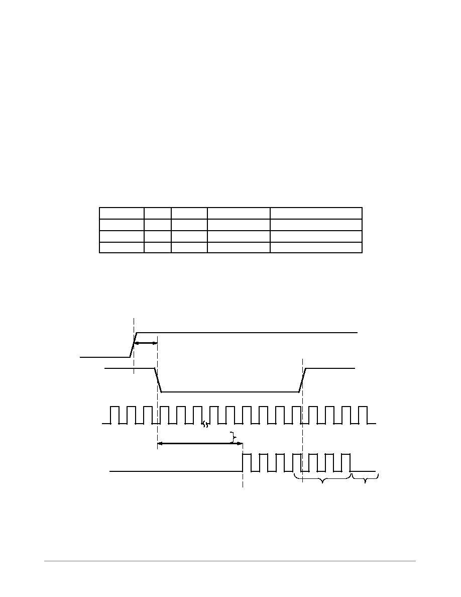
Typical Power On Sequence
1. Power On
2. Reference Clock present; must be switching before ENABLEn goes High.
3. Output Enable, ENABLEn, HightoLow
Figure 3. ENABLEn Timing Diagram
VDD Valid to ENABLEn
~50 ms, typ
ENABLEn to Output
400 Clock Cycles @ 8 kHz
200 Clock Cycles @ 4 kHz
VDD Valid
VDD
ENABLEn
REF
CLKA/B
Completed Clock
Outputs
Then Low
4 kHz or
8 kHz
12.288 MHz
Outputs Enabled
相关PDF资料 |
PDF描述 |
|---|---|
| MS3128E20-41P | CONN RCPT 41POS WALL MNT W/PINS |
| MS27467E25A19SA | CONN PLUG 19POS STRAIGHT W/SCKT |
| VI-BNJ-MY-S | CONVERTER MOD DC/DC 36V 50W |
| VI-BNH-MY-S | CONVERTER MOD DC/DC 52V 50W |
| MS27656T21B16PC | CONN RCPT 16POS WALL MNT W/PINS |
相关代理商/技术参数 |
参数描述 |
|---|---|
| NB3N3011 | 制造商:ONSEMI 制造商全称:ON Semiconductor 功能描述:3.3 V 100 MHz / 106.25 MHz PureEdge Clock Generator with LVPECL Differential Output |
| NB3N3011DTEVB | 功能描述:BOARD EVAL FOR NB3N3011 RoHS:是 类别:编程器,开发系统 >> 评估演示板和套件 系列:* 标准包装:1 系列:PCI Express® (PCIe) 主要目的:接口,收发器,PCI Express 嵌入式:- 已用 IC / 零件:DS80PCI800 主要属性:- 次要属性:- 已供物品:板 |
| NB3N3011DTG | 功能描述:时钟合成器/抖动清除器 XTAL 3.3V LVPECL CLK RoHS:否 制造商:Skyworks Solutions, Inc. 输出端数量: 输出电平: 最大输出频率: 输入电平: 最大输入频率:6.1 GHz 电源电压-最大:3.3 V 电源电压-最小:2.7 V 封装 / 箱体:TSSOP-28 封装:Reel |
| NB3N3011DTR2G | 功能描述:时钟合成器/抖动清除器 XTAL 3.3V LVPECL CLK RoHS:否 制造商:Skyworks Solutions, Inc. 输出端数量: 输出电平: 最大输出频率: 输入电平: 最大输入频率:6.1 GHz 电源电压-最大:3.3 V 电源电压-最小:2.7 V 封装 / 箱体:TSSOP-28 封装:Reel |
| NB3N3020 | 制造商:ONSEMI 制造商全称:ON Semiconductor 功能描述:3.3 V, LV-PECL/LV-CMOS Clock Multiplier |
发布紧急采购,3分钟左右您将得到回复。