参数资料
| 型号: | NB6HQ14MMNG |
| 厂商: | ON Semiconductor |
| 文件页数: | 5/11页 |
| 文件大小: | 0K |
| 描述: | IC CLK BUFF MUX 1:4 5GHZ 16-QFN |
| 标准包装: | 123 |
| 系列: | ECLinPS MAX™ |
| 类型: | 扇出缓冲器(分配),多路复用器 |
| 电路数: | 1 |
| 比率 - 输入:输出: | 1:4 |
| 差分 - 输入:输出: | 是/是 |
| 输入: | CML,LVDS,LVPECL |
| 输出: | CML |
| 频率 - 最大: | 5GHz |
| 电源电压: | 2.375 V ~ 2.625 V |
| 工作温度: | -40°C ~ 85°C |
| 安装类型: | 表面贴装 |
| 封装/外壳: | 16-VFQFN 裸露焊盘 |
| 供应商设备封装: | 16-QFN(3x3) |
| 包装: | 管件 |
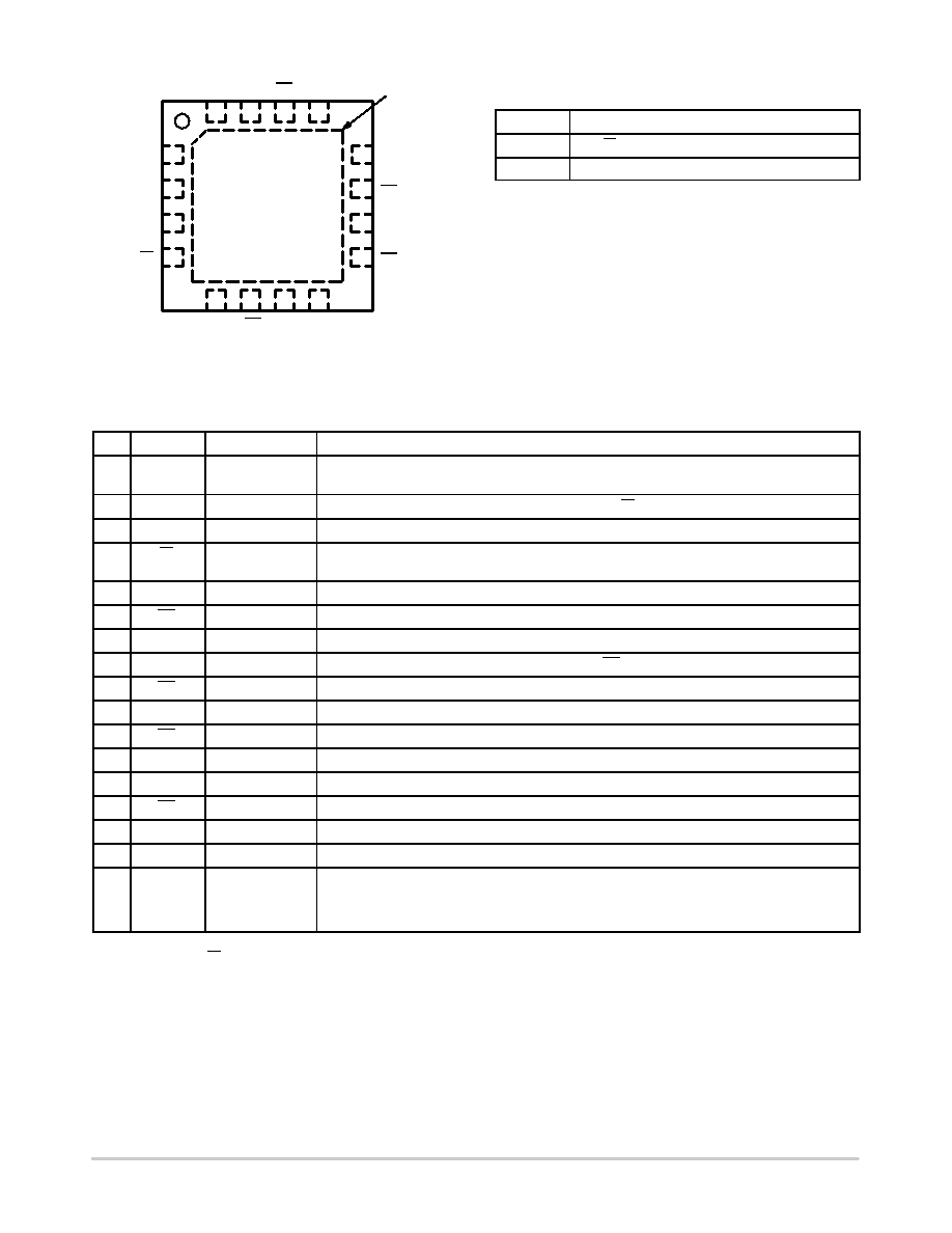
NB6HQ14M
http://onsemi.com
3
EQEN Q3
Q3 VCCO
GND Q0
Q0
VCC
Q1
Q2
IN
VT
VREFAC
IN
56
7
8
16
15
14
13
12
11
10
9
1
2
3
4
NB6HQ14M
Exposed Pad (EP)
Figure 2. QFN16 Pinout (Top View)
Table 1. EQUALIZER ENABLE FUNCTION
EQEN
Function
0
IN / IN Inputs Bypass the Equalizer section
1
Inputs flow through the Equalizer
Table 2. PIN DESCRIPTION
Pin
Name
I/O
Description
1
IN
LVPECL, CML,
LVDS Input
Noninverted Differential Input. Note 1.
2
VT
Internal 100 W Centertapped Termination Pin for IN / IN
3
VREFAC
Output Voltage Reference for CapacitorCoupled Inputs, only
4
IN
LVPECL, CML,
LVDS Input
Inverted Differential Input. Note 1.
5
EQEN
LVCMOS Input
Equalizer Enable Input; pin will default LOW when left open (has internal pulldown resistor)
6
Q3
CML Output
Inverted Differential Output. Typically Terminated with 50 W Resistor to VCC.
7
Q3
CML Output
Noninverted Differential Output. Typically Terminated with 50 W Resistor to VCC.
8
VCCO
1.8 V or 2.5 V Positive Supply Voltage for the Qn / Qn CML Outputs
9
Q2
CML Output
Inverted Differential Output. Typically Terminated with 50 W Resistor to VCC.
10
Q2
CML Output
Noninverted Differential Output. Typically Terminated with 50 W Resistor to VCC.
11
Q1
CML Output
Inverted Differential Output. Typically Terminated with 50 W Resistor to VCC.
12
Q1
CML Output
Noninverted Differential Output. Typically Terminated with 50 W Resistor to VCC.
13
VCC
2.5 V Positive Supply Voltage for the core
14
Q0
CML Output
Inverted Differential Output. Typically Terminated with 50 W Resistor to VCC.
15
Q0
CML Output
Noninverted Differential Output. Typically Terminated with 50 W Resistor to VCC.
16
GND
Negative Supply Voltage
EP
The Exposed Pad (EP) on the QFN16 package bottom is thermally connected to the die for
improved heat transfer out of package. The exposed pad must be attached to a heatsinking
conduit. The pad is electrically connected to the die, and must be electrically and thermally con-
nected to GND on the PC board.
1. In the differential configuration when the input termination pin (VT) is connected to a common termination voltage or left open, and if no signal
is applied on IN / IN input, then, the device will be susceptible to selfoscillation.
2. All VCC, VCCO and GND pins must be externally connected to a power supply for proper operation.
相关PDF资料 |
PDF描述 |
|---|---|
| NB6L11DTR2 | IC CLK BUFFER TRANSLA 1:2 8TSSOP |
| NB6L11SMNR2G | IC CLK BUFFER TRANSLA 1:2 16-QFN |
| NB6L14MNG | IC CLOCK BUFFER 1:4 3GHZ 16-QFN |
| NB6L14MNR2G | IC CLOCK BUFFER 1:4 3GHZ 16-QFN |
| NB6L14SMNTWG | IC CLK BUFFER TRANSLA 1:4 16-QFN |
相关代理商/技术参数 |
参数描述 |
|---|---|
| NB6HQ14MMNHTBG | 功能描述:缓冲器和线路驱动器 2.5V DIFF INPUT FANOUT RoHS:否 制造商:Micrel 输入线路数量:1 输出线路数量:2 极性:Non-Inverting 电源电压-最大:+/- 5.5 V 电源电压-最小:+/- 2.37 V 最大工作温度:+ 85 C 安装风格:SMD/SMT 封装 / 箱体:MSOP-8 封装:Reel |
| NB6HQ14MMNTXG | 功能描述:缓冲器和线路驱动器 2.5V DIFF INPUT FANOUT RoHS:否 制造商:Micrel 输入线路数量:1 输出线路数量:2 极性:Non-Inverting 电源电压-最大:+/- 5.5 V 电源电压-最小:+/- 2.37 V 最大工作温度:+ 85 C 安装风格:SMD/SMT 封装 / 箱体:MSOP-8 封装:Reel |
| NB6L11 | 制造商:ONSEMI 制造商全称:ON Semiconductor 功能描述:2.5V / 3.3V MULTILEVEL INPUT TO DIFFERENTIAL LVPECL/LVNECL 1:2 CLOCK OR DATA FANOUT BUFFER / TRANSLATOR |
| NB6L11_06 | 制造商:ONSEMI 制造商全称:ON Semiconductor 功能描述:2.5 V/3.3 V Multilevel Input to Differential LVPECL/LVNECL 1:2 Clock or Data Fanout Buffer/Translator |
| NB6L11D | 功能描述:时钟缓冲器 2.5V/3.3V Multilevel RoHS:否 制造商:Texas Instruments 输出端数量:5 最大输入频率:40 MHz 传播延迟(最大值): 电源电压-最大:3.45 V 电源电压-最小:2.375 V 最大功率耗散: 最大工作温度:+ 85 C 最小工作温度:- 40 C 封装 / 箱体:LLP-24 封装:Reel |
发布紧急采购,3分钟左右您将得到回复。