参数资料
| 型号: | NB6L14SMNTXG |
| 厂商: | ON Semiconductor |
| 文件页数: | 1/11页 |
| 文件大小: | 0K |
| 描述: | IC CLK BUFFER TRANSLA 1:4 16-QFN |
| 标准包装: | 3,000 |
| 系列: | AnyLevel™ |
| 类型: | 扇出缓冲器(分配),变换器 |
| 电路数: | 1 |
| 比率 - 输入:输出: | 1:4 |
| 差分 - 输入:输出: | 是/是 |
| 输入: | CML,HSCL,LVDS,LVPECL |
| 输出: | LVDS |
| 频率 - 最大: | 2GHz |
| 电源电压: | 2.375 V ~ 2.625 V |
| 工作温度: | -40°C ~ 85°C |
| 安装类型: | 表面贴装 |
| 封装/外壳: | 16-VFQFN 裸露焊盘 |
| 供应商设备封装: | 16-QFN(3x3) |
| 包装: | 带卷 (TR) |
Semiconductor Components Industries, LLC, 2011
October, 2011 Rev. 2
1
Publication Order Number:
NB6L14S/D
NB6L14S
2.5 V 1:4 AnyLevel]
Differential Input to LVDS
Fanout Buffer/Translator
The NB6L14S is a differential 1:4 Clock or Data Receiver and will
accept AnyLevel differential input signals: LVPECL, CML, LVDS, or
HSCL. These signals will be translated to LVDS and four identical
copies of Clock or Data will be distributed, operating up to 2.0 GHz or
2.5 Gb/s, respectively. As such, the NB6L14S is ideal for SONET,
GigE, Fiber Channel, Backplane and other Clock or Data distribution
applications.
The NB6L14S has a wide input common mode range from
GND + 50 mV to VCC 50 mV. Combined with the 50 W internal
termination resistors at the inputs, the NB6L14S is ideal for translating
a variety of differential or singleended Clock or Data signals to
350 mV typical LVDS output levels.
The NB6L14S is the 2.5 V version of the NB6N14S and is offered in
a small 3 mm x 3 mm 16QFN package. Application notes, models,
and support documentation are available at www.onsemi.com.
The NB6L14S is a member of the ECLinPS MAX
family of high
performance products.
Features
Maximum Input Clock Frequency > 2.0 GHz
Maximum Input Data Rate > 2.5 Gb/s
1 ps Maximum of RMS Clock Jitter
Typically 10 ps of Data Dependent Jitter
380 ps Typical Propagation Delay
120 ps Typical Rise and Fall Times
Single Power Supply; VCC = 2.5 $ 5%
VREF_AC Reference Output
These are PbFree Devices
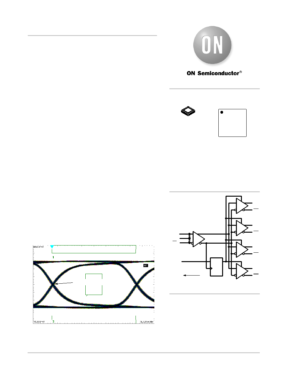
TIME (58 ps/div)
Figure 2. Typical Output Waveform at 2.488 Gb/s with
PRBS 2231 (VINPP = 400 mV; Input Signal DDJ = 14 ps)
VOL
TAGE
(130
mV/div)
Device DDJ = 10 ps
A = Assembly Location
L = Wafer Lot
Y = Year
W = Work Week
G = PbFree Package
*For additional marking information, refer to
Application Note AND8002/D.
MARKING
DIAGRAM*
QFN16
MN SUFFIX
CASE 485G
http://onsemi.com
See detailed ordering and shipping information in the package
dimensions section on page 10 of this data sheet.
ORDERING INFORMATION
16
NB6L
14S
ALYW G
G
1
1
Q3
Figure 1. Logic Diagram
Q2
Q1
Q0
EN
DQ
(LVTTL/CMOS)
VREFAC
50
W
50
W
IN
VT
IN
(Note: Microdot may be in either location)
相关PDF资料 |
PDF描述 |
|---|---|
| V48A28H500BG2 | CONVERTER MOD DC/DC 28V 500W |
| V375A3V3H264B3 | CONVERTER MOD DC/DC 3.3V 264W |
| V48A28H500BG | CONVERTER MOD DC/DC 28V 500W |
| VI-JW3-MY | CONVERTER MOD DC/DC 24V 50W |
| V48A28H500BF2 | CONVERTER MOD DC/DC 28V 500W |
相关代理商/技术参数 |
参数描述 |
|---|---|
| NB6L16 | 制造商:ONSEMI 制造商全称:ON Semiconductor 功能描述:2.5V / 3.3V Multilevel Input to Differential LVPECL/LVNECL Clock or Data Receiver/Driver/Translator Buffer |
| NB6L16_07 | 制造商:ONSEMI 制造商全称:ON Semiconductor 功能描述:2.5V / 3.3V Multilevel Input to Differential LVPECL/LVNECL Clock or Data Receiver/ Driver/Translator Buffer |
| NB6L16D | 功能描述:缓冲器和线路驱动器 2.5V/3.3V Multilevel RoHS:否 制造商:Micrel 输入线路数量:1 输出线路数量:2 极性:Non-Inverting 电源电压-最大:+/- 5.5 V 电源电压-最小:+/- 2.37 V 最大工作温度:+ 85 C 安装风格:SMD/SMT 封装 / 箱体:MSOP-8 封装:Reel |
| NB6L16DG | 功能描述:缓冲器和线路驱动器 2.5V/3.3V Multilevel to Diff LVECL RoHS:否 制造商:Micrel 输入线路数量:1 输出线路数量:2 极性:Non-Inverting 电源电压-最大:+/- 5.5 V 电源电压-最小:+/- 2.37 V 最大工作温度:+ 85 C 安装风格:SMD/SMT 封装 / 箱体:MSOP-8 封装:Reel |
| NB6L16DR2 | 功能描述:缓冲器和线路驱动器 2.5V/3.3V Multilevel RoHS:否 制造商:Micrel 输入线路数量:1 输出线路数量:2 极性:Non-Inverting 电源电压-最大:+/- 5.5 V 电源电压-最小:+/- 2.37 V 最大工作温度:+ 85 C 安装风格:SMD/SMT 封装 / 箱体:MSOP-8 封装:Reel |
发布紧急采购,3分钟左右您将得到回复。