参数资料
| 型号: | NB6L16DG |
| 厂商: | ON Semiconductor |
| 文件页数: | 1/12页 |
| 文件大小: | 0K |
| 描述: | IC CLK BUFFER DVR TRANSLA 8-SOIC |
| 标准包装: | 98 |
| 类型: | 缓冲器/驱动器,变换器 |
| 电路数: | 1 |
| 比率 - 输入:输出: | 1:1 |
| 差分 - 输入:输出: | 是/是 |
| 输入: | CML,LVCMOS,LVDS,LVNECL,LVPECL,LVTTL |
| 输出: | ECL |
| 频率 - 最大: | 6GHz |
| 电源电压: | 2.375 V ~ 3.465 V |
| 工作温度: | -40°C ~ 85°C |
| 安装类型: | 表面贴装 |
| 封装/外壳: | 8-SOIC(0.154",3.90mm 宽) |
| 供应商设备封装: | 8-SOICN |
| 包装: | 管件 |
| 其它名称: | NB6L16DG-ND NB6L16DGOS |
Semiconductor Components Industries, LLC, 2008
December, 2008 Rev. 8
1
Publication Order Number:
NB6L16/D
NB6L16
2.5V / 3.3V Multilevel Input to
Differential LVPECL/LVNECL
Clock or Data Receiver/
Driver/Translator Buffer
The NB6L16 is a high precision, low power ECL differential clock
or data receiver/driver/translator buffer. The device is functionally
equivalent to the EL16, EP16, LVEL16 and NBSG16 devices. With
output transition times of 70 ps, it is ideally suited for high frequency,
low power systems. The device is targeted for Backplane buffering,
GbE clock/data distribution, Fibre Channel distribution and SONET
clock/data distribution applications.
Input accept LVNECL (Negative ECL), LVPECL (Positive ECL),
LVTTL, LVCMOS, CML, or LVDS. Outputs are 800 mV
ECL signals.
The VBB pin, an internally generated voltage supply, is available to
this device only. For singleended input conditions, the unused
differential input is connected to VBB as a switching reference voltage.
VBB may also rebias AC coupled inputs. When used, decouple VBB
and VCC via a 0.01 mF capacitor and limit current sourcing or sinking
to 0.5 mA. When not used, VBB should be left open.
Features
Input Clock Frequency w 6 GHz
Input Data Rate Frequency w 6 Gb/s
Low 12 mA Typical Power Supply Current
70 ps Typical Rise/Fall Times
130 ps Input Propagation Delay
OnChip Reference for ECL SingleEnded Input VBB Output
PECL Mode Operating Range:
VCC = 2.375 V to 3.465 V with VEE = 0 V
NECL Mode Operating Range:
VCC = 0 V with VEE = 2.375 V to 3.465 V
Open Input Default State
LVDS, LVPECL, LVNECL, LVCMOS, LVTTL and CML Input
Compatible
PbFree Packages are Available
A
= Assembly Location
L
= Wafer Lot
Y
= Year
W
= Work Week
G
= PbFree Package
MARKING
DIAGRAMS*
6L16
ALYWG
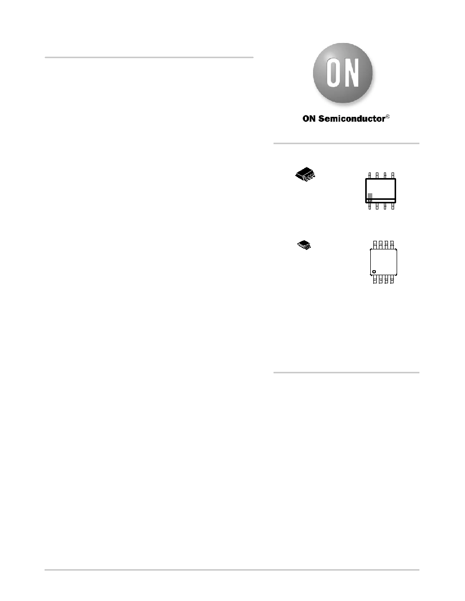
G
SOIC8
D SUFFIX
CASE 751
1
8
TSSOP8
DT SUFFIX
CASE 948R
1
8
1
8
*For additional marking information, refer to
Application Note AND8002/D.
1
8
See detailed ordering and shipping information in the package
dimensions section on page 10 of this data sheet.
ORDERING INFORMATION
http://onsemi.com
6L16
ALYW
G
(Note: Microdot may be in either location)
相关PDF资料 |
PDF描述 |
|---|---|
| V150A48H500BL | CONVERTER MOD DC/DC 48V 500W |
| VI-JTP-MY | CONVERTER MOD DC/DC 13.8V 50W |
| VE-J1R-MX-B1 | CONVERTER MINIMOD DC/DC 7.5V 75W |
| V150A48H500B3 | CONVERTER MOD DC/DC 48V 500W |
| VI-JTN-MY | CONVERTER MOD DC/DC 18.5V 50W |
相关代理商/技术参数 |
参数描述 |
|---|---|
| NB6L16DR2 | 功能描述:缓冲器和线路驱动器 2.5V/3.3V Multilevel RoHS:否 制造商:Micrel 输入线路数量:1 输出线路数量:2 极性:Non-Inverting 电源电压-最大:+/- 5.5 V 电源电压-最小:+/- 2.37 V 最大工作温度:+ 85 C 安装风格:SMD/SMT 封装 / 箱体:MSOP-8 封装:Reel |
| NB6L16DR2G | 功能描述:缓冲器和线路驱动器 2.5V/3.3V Multilevel to Diff LVECL RoHS:否 制造商:Micrel 输入线路数量:1 输出线路数量:2 极性:Non-Inverting 电源电压-最大:+/- 5.5 V 电源电压-最小:+/- 2.37 V 最大工作温度:+ 85 C 安装风格:SMD/SMT 封装 / 箱体:MSOP-8 封装:Reel |
| NB6L16DT | 功能描述:缓冲器和线路驱动器 2.5V/3.3V Multilevel RoHS:否 制造商:Micrel 输入线路数量:1 输出线路数量:2 极性:Non-Inverting 电源电压-最大:+/- 5.5 V 电源电压-最小:+/- 2.37 V 最大工作温度:+ 85 C 安装风格:SMD/SMT 封装 / 箱体:MSOP-8 封装:Reel |
| NB6L16DTG | 功能描述:缓冲器和线路驱动器 2.5V/3.3V Multilevel to Diff LVECL RoHS:否 制造商:Micrel 输入线路数量:1 输出线路数量:2 极性:Non-Inverting 电源电压-最大:+/- 5.5 V 电源电压-最小:+/- 2.37 V 最大工作温度:+ 85 C 安装风格:SMD/SMT 封装 / 箱体:MSOP-8 封装:Reel |
| NB6L16DTR2 | 功能描述:缓冲器和线路驱动器 2.5V/3.3V Multilevel RoHS:否 制造商:Micrel 输入线路数量:1 输出线路数量:2 极性:Non-Inverting 电源电压-最大:+/- 5.5 V 电源电压-最小:+/- 2.37 V 最大工作温度:+ 85 C 安装风格:SMD/SMT 封装 / 箱体:MSOP-8 封装:Reel |
发布紧急采购,3分钟左右您将得到回复。