参数资料
| 型号: | NB6L16DTR2G |
| 厂商: | ON Semiconductor |
| 文件页数: | 10/12页 |
| 文件大小: | 0K |
| 描述: | IC CLK BUFF DRIVER XLATOR 8TSSOP |
| 标准包装: | 2,500 |
| 类型: | 缓冲器/驱动器,变换器 |
| 电路数: | 1 |
| 比率 - 输入:输出: | 1:1 |
| 差分 - 输入:输出: | 是/是 |
| 输入: | CML,LVCMOS,LVDS,LVNECL,LVPECL,LVTTL |
| 输出: | ECL |
| 频率 - 最大: | 6GHz |
| 电源电压: | 2.375 V ~ 3.465 V |
| 工作温度: | -40°C ~ 85°C |
| 安装类型: | 表面贴装 |
| 封装/外壳: | 8-TSSOP,8-MSOP(0.118",3.00mm 宽) |
| 供应商设备封装: | 8-TSSOP |
| 包装: | 带卷 (TR) |
NB6L16
http://onsemi.com
7
Table 7. AC CHARACTERISTICS VCC = 0 V; VEE = 3.465 V to 2.375 V or VCC = 2.375 V to 3.465 V; VEE = 0 V (Note 24)
Symbol
Characteristic
40°C
25°C
85°C
Unit
Min
Typ
Max
Min
Typ
Max
Min
Typ
Max
VOUTPP
Output Voltage Amplitude
fin < 3 GHz
fin < 6 GHz
500
270
700
350
500
270
700
350
500
270
700
300
mV
fDATA
Maximum Operating Data Rate
6
Gb/s
tPLH,
tPHL
Propagation Delay to
Output Differential @ 1 GHz
80
130
180
80
130
180
85
135
185
ps
tSKEW
Duty Cycle Skew (Note 25)
DevicetoDevice Skew
3
30
25
60
3
30
25
60
3
30
25
60
ps
tJITTER
RMS Random Clock Jitter
(Note 26)
fin < 6 GHz
PeaktoPeak Data Dependent JItter
(Note 27)
fin < 6 Gb/s
0.2
2
1
12
0.2
2
1
12
0.2
2
1
12
ps
VINPP
Input Voltage Swing / Sensitivity
(Differential Configuration) (Note 28)
75
700
2500
75
700
2500
75
700
2500
mV
tr
tf
Output Rise/Fall Times
Q, Q
(20% 80%)
30
70
120
30
70
120
30
70
120
ps
NOTE: Device will meet the specifications after thermal equilibrium has been established when mounted in a test socket or printed circuit
board with maintained transverse airflow greater than 500 lfpm. Electrical parameters are guaranteed only over the declared
operating temperature range. Functional operation of the device exceeding these conditions is not implied. Device specification limit
values are applied individually under normal operating conditions and not valid simultaneously.
24.Measured using a 800 mV source, 50% duty cycle clock source. All loading with 50 W to VCC. Input edge rates 40 ps (20% 80%).
25.See Figure 9 tskew = |tPLH tPHL| for a nominal 50% differential clock input waveform. Skew is measured between outputs under identical
transitions and conditions @ 1 GHz.
26.Additive RMS jitter with 50% duty cycle clock signal at 6 GHz.
27.Additive PeaktoPeak data dependent jitter with NRZ PRBS 2231 data rate at 6 Gb/s.
28.VINPP(max) cannot exceed VCC VEE. (Applicable only when VCC VEE < 2500 mV). Input voltage swing is a singleended measurement
operating in the differential mode.
0.0
0.1
0.2
0.3
0.4
0.5
0.6
0.7
0.8
1
2
3
4
5
678
OUTPUT
VOL
TAGE
AMPLITUDE
(V)
INPUT CLOCK FREQUENCY (GHz)
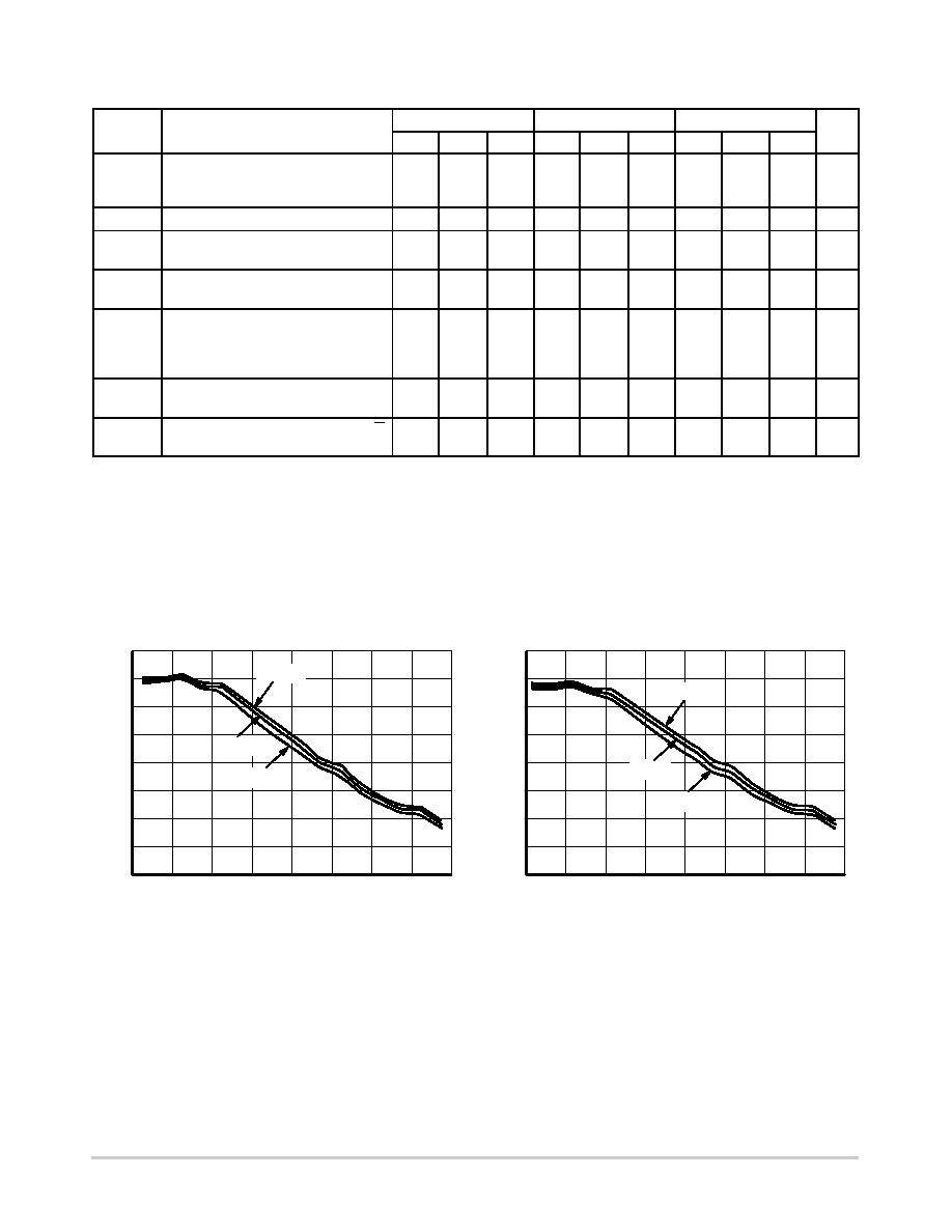
Figure 2. Output Voltage Amplitude (VOUTPP)
versus Input Clock Frequency (fIN) and
Temperature at VCC VEE = 3.3 V
0.0
0.1
0.2
0.3
0.4
0.5
0.6
0.7
0.8
12
34
5
6
7
8
INPUT CLOCK FREQUENCY (GHz)
Figure 3. Output Voltage Amplitude (VOUTPP)
versus Input Clock Frequency (fIN) and
Temperature at VCC VEE = 2.5 V
OUTPUT
VOL
TAGE
AMPLITUDE
(V)
85°C
40°C
25°C
40°C
25°C
85°C
相关PDF资料 |
PDF描述 |
|---|---|
| V150A12H500B | CONVERTER MOD DC/DC 12V 500W |
| LTC1659CMS8#TRPBF | IC D/A CONV 12BIT R-R 8-MSOP |
| V375A12H400BF2 | CONVERTER MOD DC/DC 12V 400W |
| LTC1659CMS8#TR | IC DAC 12BIT R-R MICROPWR 8MSOP |
| V48A48H500BG2 | CONVERTER MOD DC/DC 48V 500W |
相关代理商/技术参数 |
参数描述 |
|---|---|
| NB6L239 | 制造商:ONSEMI 制造商全称:ON Semiconductor 功能描述:2.5V / 3.3V Any Differential Clock IN to Differential LVPECL OUT /1/2/4/8, /2/4/8/16 Clock Divider |
| NB6L239_06 | 制造商:ONSEMI 制造商全称:ON Semiconductor 功能描述:2.5V / 3.3V Any Differential Clock IN to Differential LVPECL OUT /1/2/4/8, /2/4/8/16 Clock Divider |
| NB6L239MN | 功能描述:时钟驱动器及分配 2.5V/3.3V LVPECL Out RoHS:否 制造商:Micrel 乘法/除法因子:1:4 输出类型:Differential 最大输出频率:4.2 GHz 电源电压-最大: 电源电压-最小:5 V 最大工作温度:+ 85 C 封装 / 箱体:SOIC-8 封装:Reel |
| NB6L239MNEVB | 功能描述:BOARD EVAL BBG NB6L239MND RoHS:是 类别:编程器,开发系统 >> 评估演示板和套件 系列:* 标准包装:1 系列:PCI Express® (PCIe) 主要目的:接口,收发器,PCI Express 嵌入式:- 已用 IC / 零件:DS80PCI800 主要属性:- 次要属性:- 已供物品:板 |
| NB6L239MNG | 功能描述:时钟驱动器及分配 2.5V/3.3V LVPECL Out Dual Bank RoHS:否 制造商:Micrel 乘法/除法因子:1:4 输出类型:Differential 最大输出频率:4.2 GHz 电源电压-最大: 电源电压-最小:5 V 最大工作温度:+ 85 C 封装 / 箱体:SOIC-8 封装:Reel |
发布紧急采购,3分钟左右您将得到回复。