参数资料
| 型号: | NB6L239MNEVB |
| 厂商: | ON Semiconductor |
| 文件页数: | 2/6页 |
| 文件大小: | 0K |
| 描述: | BOARD EVAL BBG NB6L239MND |
| 设计资源: | NB6L239MNEVB Gerber Files |
| 标准包装: | 1 |
| 系列: | * |
�� �
�
�NB6L239MNEVB�
�PROCEDURE�
�Lab� Setup� and� Measurement� Procedure�
�Dual� Power� Supplies�
�Equipment� Used�
�?� Agilent� Signal� Generator� #8133A�
�?� Tektronix� TDS8000� Oscilloscope�
�?� Agilent� #6624A� DC� Power� Supply�
�?� Digital� Voltmeter�
�?� Matched� High� ?� Speed� Cables� with� SMA� Connectors�
�Power� Supply� Connections�
�+�
�V� CC�
�+2.0� V�
�?�
�V� TT�
�+1.3� V�
�+�
�?�
�V� EE�
�The� NB6L239� has� a� positive� supply� pin,� V� CC� ,� and� a�
�negative� supply� pin,� V� EE� .� SMAGND� =� V� TT� =� V� CC� –� 2.0� V�
�is� the� termination� supply� for� the� LVPECL� outputs,� only.�
�Power� supply� terminals� V� CC� ,� V� EE� and� SMAGND� are�
�provided.� The� SMAGND� terminal� is� for� the� isolated� SMA�
�connector� GROUND� plane,� and� is� not� to� be� confused� with�
�a� device� V� EE� pin.� Since� SMAGND� =� V� TT� =� V� CC� –� 2.0� V,� is�
�the� termination� supply� for� the� LVPECL� outputs,� by�
�offsetting� V� CC� by� +2.0� V� yields� V� TT� =� 0� V� or� Ground.� A�
�“split”� or� dual� power� supply� technique� can� be� used� to� take�
�advantage� of� terminating� the� PECL� outputs� into� 50� W� to�
�Ground� of� an� oscilloscope� or� a� frequency� counter.�
�(see� AND8020/D� for� more� information� on�
�terminating� ECL).�
�Table� 1.� POWER� SUPPLY� CONFIGURATIONS�
�Power� Supply�
�Device� Connector�
�Pin� Color� “Spilt”� Power� Supply�
�V� CC� RED� V� CC� =� +2.0� V�
�?� BLACK� ?� V� TT� =� V� CC� –� 2� V� =� 0� V�
�SMAGND�
�V� EE� –� 239� YELLOW� V� EE� =� ?� 1.3� V� (or� –0.5� V)�
�+3.3� V�
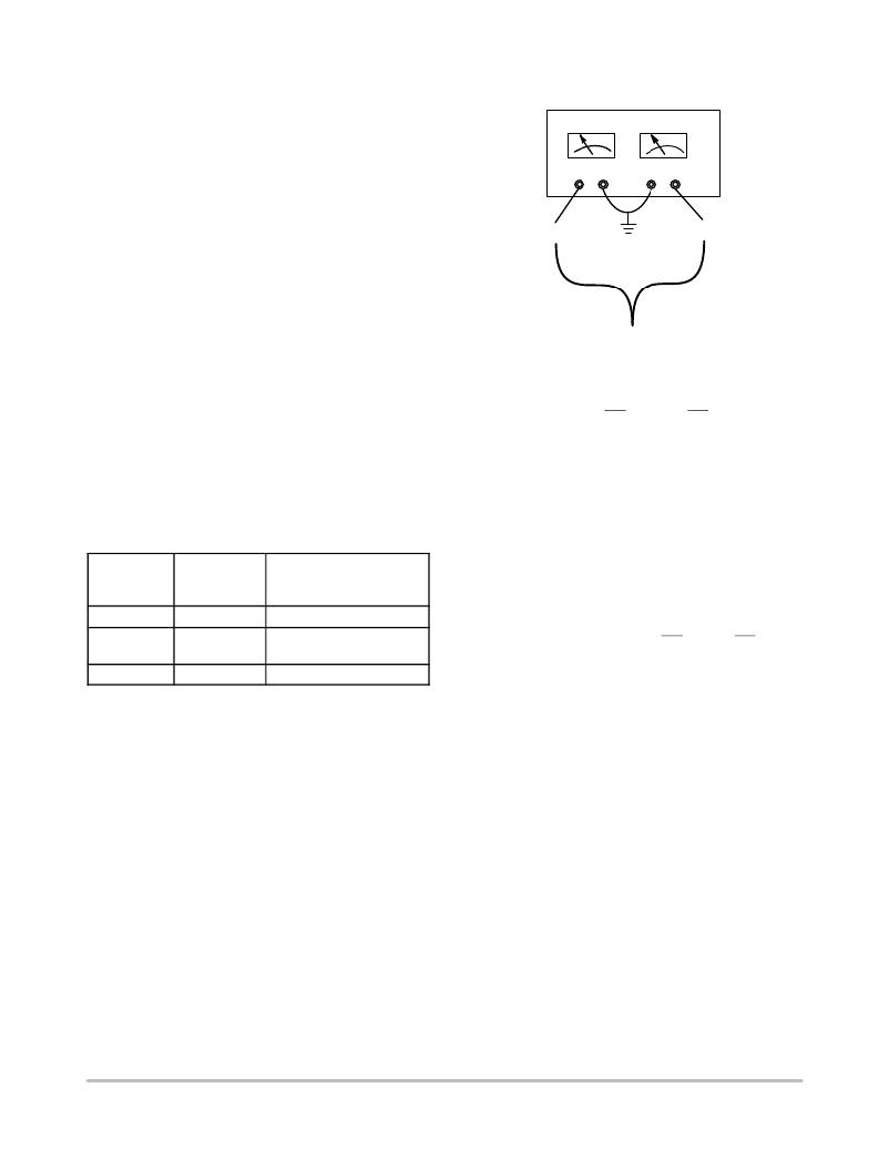
�Figure� 2.� “Split”� or� Dual� Power� Supply� Connections�
�NB6L239�
�To� monitor� the� QA/QA� and� QB/QB� outputs� on� an�
�oscilloscope,� the� power� supply� needs� to� be� DC� offset:�
�1.� Connect� a� “split”� power� supply� to� the� evaluation�
�board.� (Figure� 1)�
�Connect� V� CC� to� +2.0� V�
�Connect� SMAGND� to� 0� V�
�Connect� V� EE� to� ?� 1.3� V� for� 3.3� V� operation;� or�
�–0.5� V� for� 2.5� V� operation�
�2.� Ensure� the� oscilloscope� is� triggered� properly� and�
�has� 50� W� termination� to� ground.� The� board� does�
�not� provide� 50� W� source� termination� resistors.�
�Trigger� the� oscilloscope� from� trigger� output� of�
�signal� generator.�
�3.� Connect� the� LVPECL� QA/QA� and� QB/QB� outputs�
�to� the� oscilloscope� with� matched� cables.� The�
�outputs� are� terminated� with� 50� W� to� V� TT�
�(V� CC� –� 2.0� V)� =� 0� V� =� Ground� internal� to�
�the� oscilloscope.�
�http://onsemi.com�
�2�
�相关PDF资料 |
PDF描述 |
|---|---|
| NB7L32MMNEVB | BOARD EVAL FOR NB7L32MM |
| NB7N017MEVB | BOARD EVAL BBG NB7N017MMN |
| NC2003SR | STAND NOTEBOOK W/2FANS USB |
| NCN9252MUGEVB | BOARD EVALUATION NCN9252MU |
| NCP1031POEEVB | BOARD EVAL NCP1031 POE DC CONV |
相关代理商/技术参数 |
参数描述 |
|---|---|
| NB6L239MNG | 功能描述:时钟驱动器及分配 2.5V/3.3V LVPECL Out Dual Bank RoHS:否 制造商:Micrel 乘法/除法因子:1:4 输出类型:Differential 最大输出频率:4.2 GHz 电源电压-最大: 电源电压-最小:5 V 最大工作温度:+ 85 C 封装 / 箱体:SOIC-8 封装:Reel |
| NB6L239MNR2 | 功能描述:时钟驱动器及分配 2.5V/3.3V LVPECL Out RoHS:否 制造商:Micrel 乘法/除法因子:1:4 输出类型:Differential 最大输出频率:4.2 GHz 电源电压-最大: 电源电压-最小:5 V 最大工作温度:+ 85 C 封装 / 箱体:SOIC-8 封装:Reel |
| NB6L239MNR2G | 功能描述:时钟驱动器及分配 2.5V/3.3V LVPECL Out Dual Bank RoHS:否 制造商:Micrel 乘法/除法因子:1:4 输出类型:Differential 最大输出频率:4.2 GHz 电源电压-最大: 电源电压-最小:5 V 最大工作温度:+ 85 C 封装 / 箱体:SOIC-8 封装:Reel |
| NB6L295 | 制造商:ONSEMI 制造商全称:ON Semiconductor 功能描述:2.5V / 3.3V Dual Channel Programmable Clock/Data Delay with Differential LVPECL Outputs |
| NB6L295M | 制造商:ONSEMI 制造商全称:ON Semiconductor 功能描述:2.5V / 3.3V Dual Channel Programmable Clock/Data Delay with Differential CML Outputs |
发布紧急采购,3分钟左右您将得到回复。