参数资料
| 型号: | NB6L295MMNTXG |
| 厂商: | ON Semiconductor |
| 文件页数: | 7/13页 |
| 文件大小: | 0K |
| 描述: | IC DELAY LINE 511TAP 24-QFN |
| 标准包装: | 3,000 |
| 标片/步级数: | 512 |
| 功能: | 多重,可编程 |
| 延迟到第一抽头: | 3.2ns,6.2ns |
| 接头增量: | 11ps |
| 可用的总延迟: | 3.2ns ~ 8.5ns,6.2ns ~ 16.6ns |
| 独立延迟数: | 2 |
| 电源电压: | 2.375 V ~ 3.6 V |
| 工作温度: | -40°C ~ 85°C |
| 安装类型: | 表面贴装 |
| 封装/外壳: | 24-VFQFN 裸露焊盘 |
| 供应商设备封装: | 24-QFN(4x4) |
| 包装: | 带卷 (TR) |
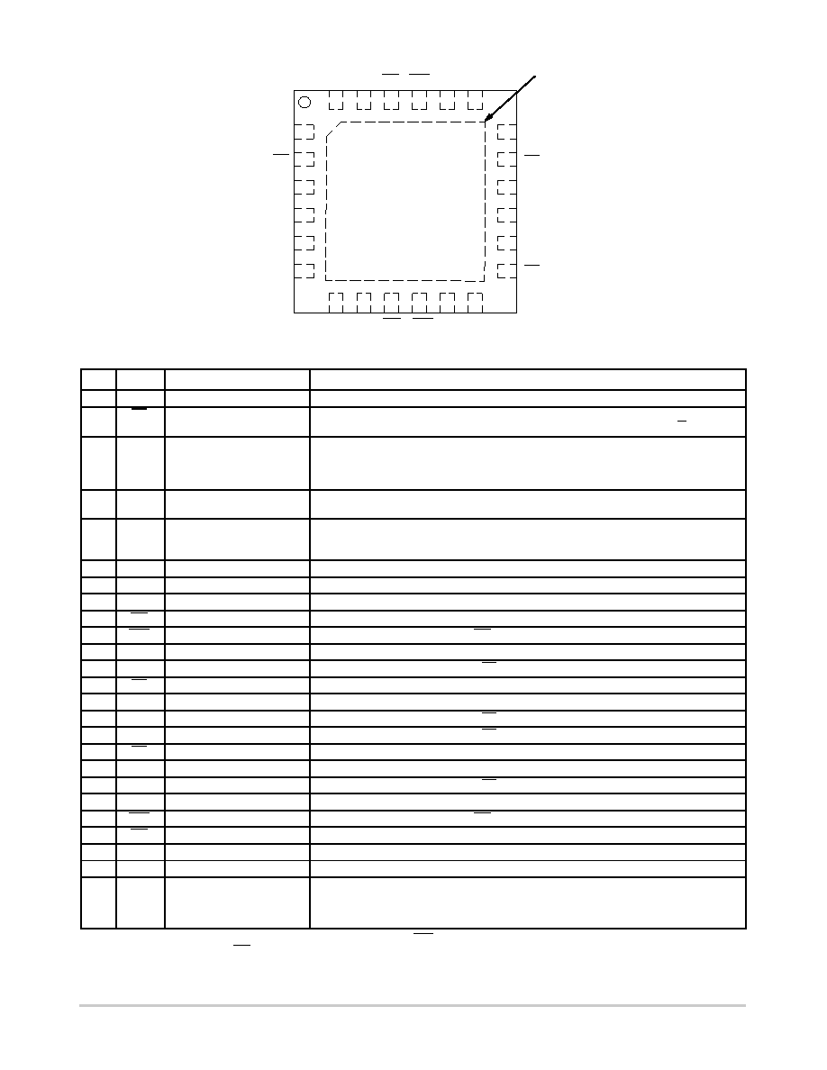
NB6L295M
http://onsemi.com
3
SDIN
SLOAD
VCC
VT1
VCC0
Q0
VCC0
VCC1
Q1
VCC1
GND
VT1
VCC
GND
EN
SCLK
IN0
IN1
IN0
Q1
Q0
VT0
NB6L295M
18
12
4
3
5
6
78
9
11
10
2
1
17
16
15
14
13
19
24
23
22
20
21
Exposed Pad
(EP)
Figure 2. Pinout: QFN24 (Top View)
VT0
Table 1. PIN DESCRIPTION
Pin
Name
I/O
Description
1
VCC
Power Supply
Positive Supply Voltage for the Inputs and Core Logic
2
EN
LVCMOS/LVTTL Input
Input Enable/ Disable for both PD0 and PD1. LOW for enable, HIGH for disable, Open
Pin Default state LOW (37 kW Pulldown Resistor). High Forces Q LOW and Q HIGH.
3
SLOAD
LVCMOS/LVTTL Input
Serial Load; This pin loads the configuration latches with the contents of the shift
register. The latches will be transparent when this signal is HIGH; thus, the data must be
stable on the HIGHtoLOW transition of S_LOAD for proper operation. Open Pin
Default state LOW (37 kW Pulldown Resistor).
4
SDIN
LVCMOS/LVTTL Input
Serial Data In; This pin acts as the data input to the serial configuration shift register.
Open Pin Default state LOW (37 kW Pulldown Resistor).
5
SCLK
LVCMOS/LVTTL Input
Serial Clock In; This pin serves to clock the serial configuration shift register. Data from
SDIN is sampled on the rising edge. Open Pin Default state LOW (37 kW Pulldown
Resistor).
6
VCC
Power Supply
Positive Supply Voltage for the Inputs and Core Logic
7
VT1
Internal 50 W Termination Pin for IN1.
8
IN1
LVPECL, CML, LVDS Input
Noninverted differential input. Note 1. Channel 1.
9
IN1
LVPECL, CML, LVDS Input
Inverted differential input. Note 1. Channel 1.
10
VT1
Internal 50 W Termination Pin for IN1
11
GND
Power Supply
Negative Power Supply
12
VCC1
Power Supply
Positive Supply Voltage for the Q1/Q1 outputs, channel PD1
13
Q1
CML Output
Inverted Differential Output. Channel 1. Typically terminated with 50 W resistor to VCC1
14
Q1
CML Output
Noninverted Differential Output. Channel 1. Typically terminated with 50 W resistor to VCC1
15
VCC1
Power Supply
Positive Supply Voltage for the Q1/Q1 outputs, channel PD1
16
VCC0
Power Supply
Positive Supply Voltage for the Q0/Q0 outputs, channel PD0
17
Q0
CML Output
Inverted Differential Output. Channel 0. Typically terminated with 50 W resistor to VCC0
18
Q0
CML Output
Noninverted Differential Output. Channel 0. Typically terminated with 50 W resistor to VCC0
19
VCC0
Power Supply
Positive Supply Voltage for the Q0/Q0 outputs, channel PD0
20
GND
Power Supply
Negative Power Supply
21
VT0
Internal 50 W Termination Pin for IN0
22
IN0
LVPECL, CML, LVDS Input
Inverted differential input. Note 1. Channel 0.
23
IN0
LVPECL, CML, LVDS Input
Noninverted differential input. Note 1. Channel 0.
24
VT0
Internal 50 W Termination Pin for IN0
EP
Ground
The Exposed Pad (EP) on the QFN24 package bottom is thermally connected to the
die for improved heat transfer out of package. The exposed pad must be attached to a
heatsinking conduit. The pad is electrically connected to GND and must be connected
to GND on the PC board.
1. In the differential configuration when the input termination pin (VTx/VTx) are connected to a common termination voltage or left open, and
if no signal is applied on INx/INx input then the device will be susceptible to selfoscillation.
2. All VCC, VCC0 and VCC1 Pins must be externally connected to the same power supply for proper operation. Both VCC0s are connected
to each other and both VCC1s are connected to each other: VCC0 and VCC1 are separate.
相关PDF资料 |
PDF描述 |
|---|---|
| NB6L295MNTXG | IC DELAY LINE 511TAP 24-QFN |
| NBVSBA017LNHTAG | IC OSC VCXO 156.25MHZ 6CLCC |
| NBVSBA041LNHTAG | IC VCXO LVPECL 693.4830MHZ 6CLCC |
| NBVSPA013LNHTAG | IC VCXO LVDS 212MHZ 6CLCC |
| NBVSPA024LNHTAG | IC VCXO LVDS 160MHZ 6CLCC |
相关代理商/技术参数 |
参数描述 |
|---|---|
| NB6L295MNG | 功能描述:延迟线/计时元素 LVPECL DUAL PRG DLAY RoHS:否 制造商:Micrel 功能:Active Programmable Delay Line 传播延迟时间:1000 ps 工作温度范围: 封装 / 箱体:QFN-24 封装:Tube |
| NB6L295MNGEVB | 功能描述:电源管理IC开发工具 NB6L295 EVAL BOARD RoHS:否 制造商:Maxim Integrated 产品:Evaluation Kits 类型:Battery Management 工具用于评估:MAX17710GB 输入电压: 输出电压:1.8 V |
| NB6L295MNTXG | 功能描述:延迟线/计时元素 LVPECL DUAL PRG DLAY RoHS:否 制造商:Micrel 功能:Active Programmable Delay Line 传播延迟时间:1000 ps 工作温度范围: 封装 / 箱体:QFN-24 封装:Tube |
| NB6L56MNG | 功能描述:时钟缓冲器 TSMC 2.5V/3.3V DUAL DIFF RoHS:否 制造商:Texas Instruments 输出端数量:5 最大输入频率:40 MHz 传播延迟(最大值): 电源电压-最大:3.45 V 电源电压-最小:2.375 V 最大功率耗散: 最大工作温度:+ 85 C 最小工作温度:- 40 C 封装 / 箱体:LLP-24 封装:Reel |
| NB6L56MNTXG | 功能描述:时钟缓冲器 2.5V/3.3V DUAL DIFFERENTI RoHS:否 制造商:Texas Instruments 输出端数量:5 最大输入频率:40 MHz 传播延迟(最大值): 电源电压-最大:3.45 V 电源电压-最小:2.375 V 最大功率耗散: 最大工作温度:+ 85 C 最小工作温度:- 40 C 封装 / 箱体:LLP-24 封装:Reel |
发布紧急采购,3分钟左右您将得到回复。