参数资料
| 型号: | NB6L611MNR2G |
| 厂商: | ON Semiconductor |
| 文件页数: | 1/10页 |
| 文件大小: | 0K |
| 描述: | IC CLOCK BUFFER 1:2 4GHZ 16-QFN |
| 标准包装: | 1 |
| 系列: | ECLinPS MAX™ |
| 类型: | 扇出缓冲器(分配) |
| 电路数: | 1 |
| 比率 - 输入:输出: | 1:2 |
| 差分 - 输入:输出: | 是/是 |
| 输入: | CML,LVCMOS,LVDS,LVPECL,LVTTL |
| 输出: | LVPECL |
| 频率 - 最大: | 4GHz |
| 电源电压: | 2.375 V ~ 3.63 V |
| 工作温度: | -40°C ~ 85°C |
| 安装类型: | 表面贴装 |
| 封装/外壳: | 16-VFQFN 裸露焊盘 |
| 供应商设备封装: | 16-QFN(3x3) |
| 包装: | 剪切带 (CT) |
| 其它名称: | NB6L611MNR2GOSCT |
Semiconductor Components Industries, LLC, 2009
August, 2009 Rev. 4
1
Publication Order Number:
NB6L611/D
NB6L611
2.5V / 3.3V 1:2 Differential
LVPECL Clock / Data Fanout
Buffer
MultiLevel Inputs with Internal Termination
Description
The NB6L611 is a differential 1:2 clock or data fanout buffer. The
differential inputs incorporate internal 50
W termination resistors that
are accessed through the VTD pins and will accept LVPECL, CML,
LVDS, LVCMOS or LVTTL logic levels.
The VREFAC reference output can be used to rebias
capacitorcoupled differential or singleended input signals. When
used, decouple VREFAC with a 0.01 mF capacitor and limit current
sourcing or sinking to 0.5 mA. When used, decouple VREFAC with a
0.01
mF capacitor and limit current sourcing or sinking to 0.5 mA.
When not used, VREFAC output should be left open.
The device is housed in a small 3x3 mm 16 pin QFN package.
The NB6L611 is a member of the ECLinPS MAX
family of high
performance clock and data management products.
Features
Input Clock Frequency > 4.0 GHz
280 ps Typical Propagation Delay
100 ps Typical Rise and Fall Times
0.5 ps maximum RMS Clock Jitter
Differential LVPECL Outputs, 780 mV Amplitude, typical
LVPECL Operating Range: VCC = 2.375 V to 3.63 V with VEE = 0 V
NECL Operating Range: VCC = 0 V with VEE = 2.375 V to 3.63 V
Internal Input Termination Resistors, 50 W
VREFAC Reference Output Voltage
Functionally Compatible with Existing 2.5 V / 3.3 V LVEL, LVEP,
EP, and SG Devices
40°C to +85°C Ambient Operating Temperature
These are PbFree Devices
MARKING
DIAGRAM*
http://onsemi.com
QFN16
MN SUFFIX
CASE 485G
NB6L
611
ALYWG
G
A
= Assembly Location
L
= Wafer Lot
Y
= Year
W
= Work Week
G
= PbFree Package
(Note: Microdot may be in either location)
16
1
*For additional marking information, refer to
Application Note AND8002/D.
See detailed ordering and shipping information in the package
dimensions section on page 9 of this data sheet.
ORDERING INFORMATION
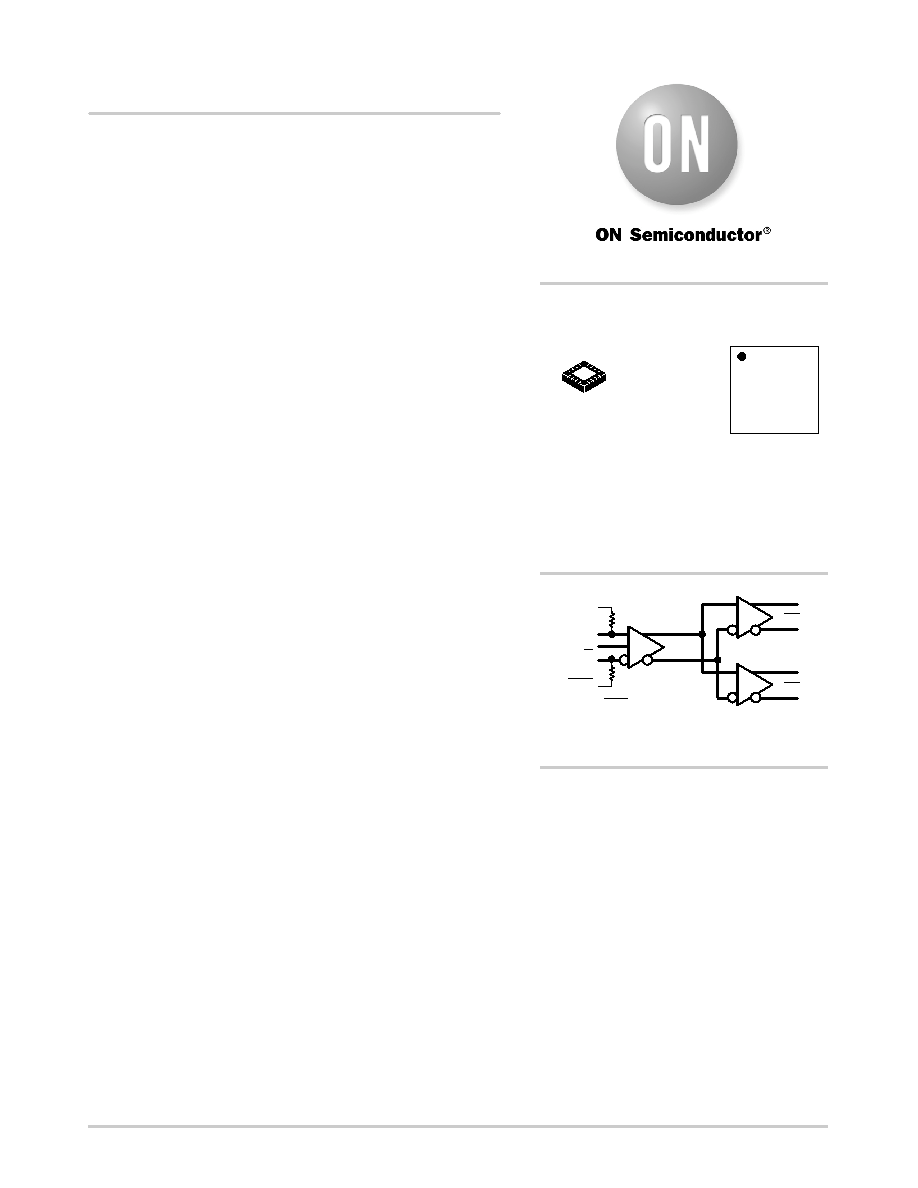
Figure 1. Simplified Logic Diagram
Q0
Q1
D
VTD
VREFAC
1
相关PDF资料 |
PDF描述 |
|---|---|
| NB6LQ572MMNG | IC CLK BUFFER MUX TRANSLA 32-QFN |
| NB6LQ572MNG | IC CLOCK MUX TRANSLA 4:2 32-QFN |
| NB6N11SMNR2G | IC CLK BUFFER TRANSLA 1:2 16-QFN |
| NB6N14SMNR2G | IC CLK BUFFER TRANSLA 1:4 16-QFN |
| NB6VQ572MMNG | IC CLOCK MUX TRANSLA 4:2 32-QFN |
相关代理商/技术参数 |
参数描述 |
|---|---|
| NB6L72 | 制造商:ONSEMI 制造商全称:ON Semiconductor 功能描述:2.5V / 3.3V Differential 2 X 2 Crosspoint Switch with LVPECL Outputs |
| NB6L72M | 制造商:ONSEMI 制造商全称:ON Semiconductor 功能描述:2.5V / 3.3V Differential 2 X 2 Crosspoint Switch with CML Outputs |
| NB6L72M_07 | 制造商:ONSEMI 制造商全称:ON Semiconductor 功能描述:2.5V / 3.3V Differential 2 X 2 Crosspoint Switch with CML Outputs |
| NB6L72MMMNG | 制造商:ONSEMI 制造商全称:ON Semiconductor 功能描述:2.5V / 3.3V Differential 2 X 2 Crosspoint Switch with CML Outputs |
| NB6L72MMMNR2G | 制造商:ONSEMI 制造商全称:ON Semiconductor 功能描述:2.5V / 3.3V Differential 2 X 2 Crosspoint Switch with CML Outputs |
发布紧急采购,3分钟左右您将得到回复。