- 您现在的位置:买卖IC网 > PDF目录11418 > NB6L72MNG (ON Semiconductor)IC CROSSPOINT SWITCH 2X2 16QFN PDF资料下载
参数资料
| 型号: | NB6L72MNG |
| 厂商: | ON Semiconductor |
| 文件页数: | 5/11页 |
| 文件大小: | 0K |
| 描述: | IC CROSSPOINT SWITCH 2X2 16QFN |
| 标准包装: | 123 |
| 功能: | 交叉点开关 |
| 电路: | 1 x 2:2 |
| 电压电源: | 单电源 |
| 电压 - 电源,单路/双路(±): | 2.3 V ~ 3.6 V |
| 电流 - 电源: | 80mA |
| 工作温度: | -40°C ~ 85°C |
| 安装类型: | 表面贴装 |
| 封装/外壳: | 16-VFQFN 裸露焊盘 |
| 供应商设备封装: | 16-QFN(3x3) |
| 包装: | 管件 |
| 其它名称: | NB6L72MNG-ND NB6L72MNGOS |
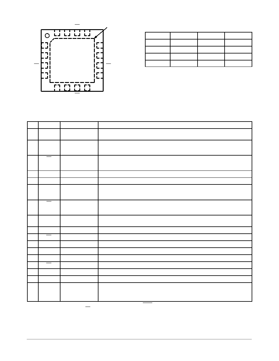
NB6L72
http://onsemi.com
3
VTD1
D1
SEL1
GND
Q0
VCC
Q1
GND
SEL0
D0
VTD0
5
678
16
15
14
13
12
11
10
9
1
2
3
4
NB6L72
Exposed Pad (EP)
Figure 2. Pin Configuration (Top View)
Table 1. INPUT/OUTPUT SELECT TRUTH TABLE
SEL0*
SEL1*
Q0
Q1
L
D0
H
L
D1
D0
L
H
D0
D1
H
D1
*Defaults HIGH when left open
Table 2. PIN DESCRIPTION
Pin
Name
I/O
Description
1
SEL0
LVTTL, LVCMOS
Input
Select Logic Input control that selects D0 or D1 to output Q0. See Table 1, Select Input
Function Table. Pin defaults HIGH when left open
2
D0
LVPECL, CML,
LVDS, LVTTL,
LVCMOS, Input
Noninverted Differential Input. Note 1.
3
D0
LVPECL, CML,
LVDS, LVTTL,
LVCMOS, Input
Inverted Differential Input. Note 1.
4
VTD0
-
Internal 50
W Termination Pin. Note 1.
5
VTD1
-
Internal 50
W termination pin. Note 1.
6
D1
LVPECL, CML,
LVDS, LVTTL,
LVCMOS, Input
Noninverted Differential Input. Note 1.
7
D1
LVPECL, CML,
LVDS, LVTTL,
LVCMOS, Input
Inverted Differential Input. Note 1.
8
SEL1
LVTTL,LVCMOS
Input
Select Logic Input control that selects D0 or D1 to output Q1. See Table 1, Select Input
Function Table. Pin defaults HIGH when left open
9
GND
-
Negative Supply Voltage
10
Q1
LVPECL Output
Inverted Differential Output. Typically Terminated with 50
W Resistor to VCC - 2.0 V.
11
Q1
LVPECL Output
Noninverted Differential Output. Typically Terminated with 50
W Resistor to VCC - 2.0 V.
12
VCC
-
Positive Supply Voltage
13
VCC
-
Positive Supply Voltage
14
Q0
LVPECL Output
Inverted Differential Reset Input. Typically Terminated with 50
W Resistor to VCC - 2.0 V.
15
Q0
LVPECL Output
Noninverted Differential Reset Input. Typically Terminated with 50
W Resistor to VCC - 2.0 V.
16
GND
-
Negative Supply Voltage
-
EP
-
The Exposed Pad (EP) on the QFN-16 package bottom is thermally connected to the die for
improved heat transfer out of package. The exposed pad must be attached to a heat-sinking
conduit. The pad is not electrically connected to the die, but is recommended to be
electrically and thermally connected to GND on the PC board.
1. In the differential configuration when the input termination pin (VTDn, VTDn) are connected to a common termination voltage or left open,
and if no signal is applied on Dn/Dn input, then the device will be susceptible to self-oscillation.
2. All VCC and GND pins must be externally connected to a power supply for proper operation.
相关PDF资料 |
PDF描述 |
|---|---|
| VI-B3Z-IY | CONVERTER MOD DC/DC 2V 20W |
| GRM2197U2A6R5DD01D | CAP CER 6.5PF 100V U2J 0805 |
| VI-B3Z-IX | CONVERTER MOD DC/DC 2V 30W |
| GRM2197U2A6R3DD01D | CAP CER 6.3PF 100V U2J 0805 |
| VI-B3Y-IY | CONVERTER MOD DC/DC 3.3V 33W |
相关代理商/技术参数 |
参数描述 |
|---|---|
| NB6L72MNGEVB | 功能描述:BOARD EVAL NB6L72MNG RoHS:是 类别:编程器,开发系统 >> 评估演示板和套件 系列:* 标准包装:1 系列:PCI Express® (PCIe) 主要目的:接口,收发器,PCI Express 嵌入式:- 已用 IC / 零件:DS80PCI800 主要属性:- 次要属性:- 已供物品:板 |
| NB6L72MNR2G | 功能描述:模拟和数字交叉点 IC 2X2 PECL CROSSPOINT RoHS:否 制造商:Micrel 配置:2 x 2 封装 / 箱体:MLF-16 数据速率:10.7 Gbps 输入电平:CML, LVDS, LVPECL 输出电平:CML 电源电压-最大:3.6 V 电源电压-最小:2.375 V 最大工作温度:+ 85 C 最小工作温度:- 40 C 产品:Digital Crosspoint 封装:Tube |
| NB6LQ572 | 制造商:ONSEMI 制造商全称:ON Semiconductor 功能描述:2.5V / 3.3V Differential 4:1 Mux w/Input Equalizer to 1:2 LVPECL Clock/Data Fanout / Translator |
| NB6LQ572M | 制造商:ONSEMI 制造商全称:ON Semiconductor 功能描述:2.5V / 3.3V Differential 4:1 Mux w/Input Equalizer to 1:2 CML Clock/Data Fanout / Translator |
| NB6LQ572MMNG | 功能描述:时钟驱动器及分配 DUAL OCP RoHS:否 制造商:Micrel 乘法/除法因子:1:4 输出类型:Differential 最大输出频率:4.2 GHz 电源电压-最大: 电源电压-最小:5 V 最大工作温度:+ 85 C 封装 / 箱体:SOIC-8 封装:Reel |
发布紧急采购,3分钟左右您将得到回复。