参数资料
| 型号: | NB7L111MMNG |
| 厂商: | ON Semiconductor |
| 文件页数: | 7/13页 |
| 文件大小: | 0K |
| 描述: | IC CLK/DATA BUFF MUX 2:10 52-QFN |
| 标准包装: | 260 |
| 类型: | 扇出缓冲器(分配),多路复用器,数据 |
| 电路数: | 1 |
| 比率 - 输入:输出: | 2:10 |
| 差分 - 输入:输出: | 是/是 |
| 输入: | CML,LVCMOS,LVDS,LVNECL,LVPECL,LVTTL |
| 输出: | CML |
| 频率 - 最大: | 5.5GHz |
| 电源电压: | 2.375 V ~ 3.465 V |
| 工作温度: | -40°C ~ 85°C |
| 安装类型: | 表面贴装 |
| 封装/外壳: | 52-VFQFN 裸露焊盘 |
| 供应商设备封装: | 52-QFN(8x8) |
| 包装: | 管件 |
| 其它名称: | NB7L111MMNG-ND NB7L111MMNGOS |
NB7L111M
http://onsemi.com
3
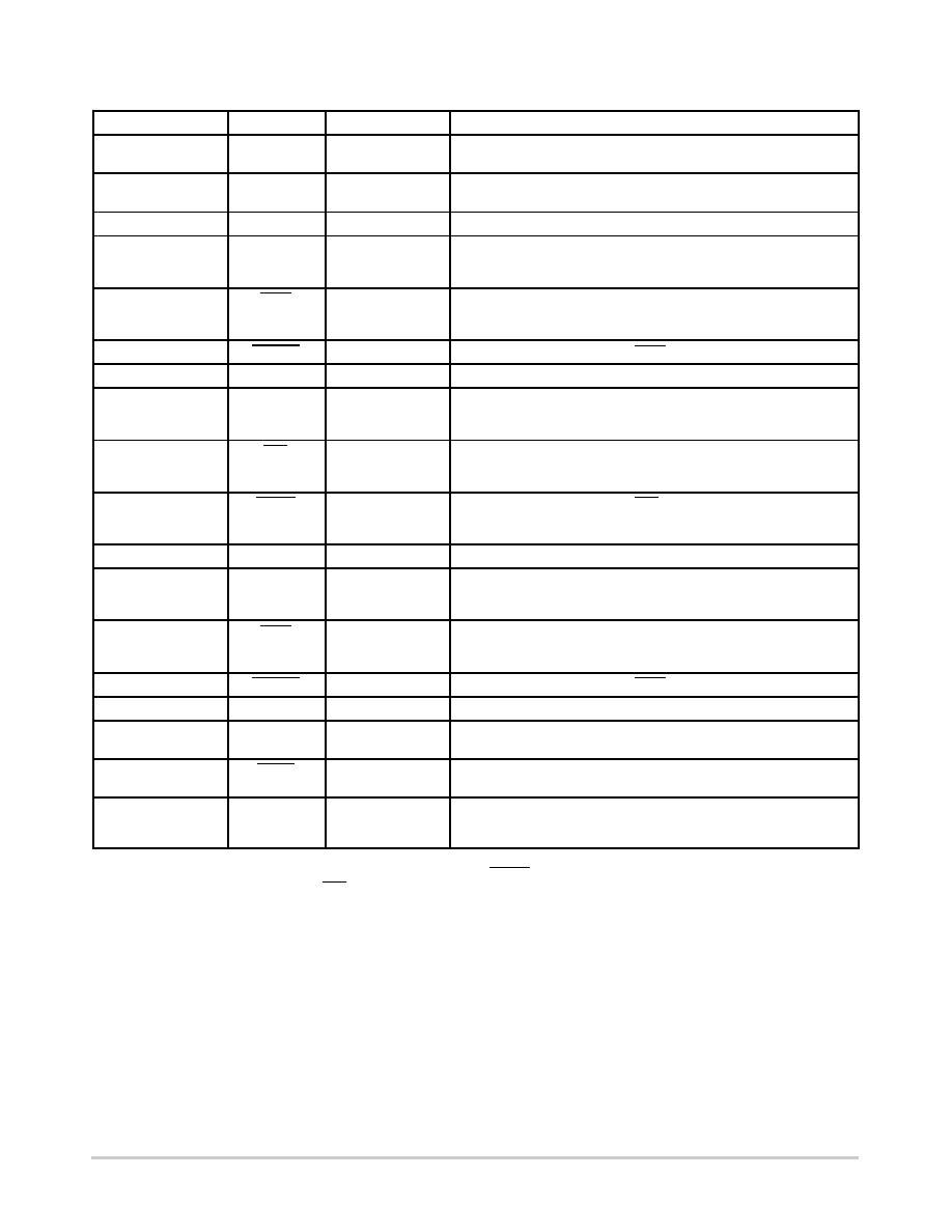
Table 2. PIN DESCRIPTION
Pin
Name
I/O
Description
15, 24, 27, 39, 42, 51
VCC
Positive supply voltage. All VCC pins must be externally connected to
power supply to guarantee proper operation.
1, 18, 21, 26, 30, 33,
36, 40, 45, 48
VEE
Negative supply voltage. All VEE pins must be externally connected to
power supply to guarantee proper operation.
2
VTCLK0
Internal 50 W termination pin for CLK0. (Note 2)
3
CLK0
LVPECL, CML,
LVCMOS, LVTTL,
LVDS Input
Noninverted differential clock/data input 0 (Note 2).
4
CLK0
LVPECL, CML,
LVCMOS, LVTTL,
LVDS Input
Inverted differential clock/data input 0 (Note 2).
5
VTCLK0
Internal 50 W termination pin for CLK0. (Note 2)
6
VTSEL
Internal 50 W termination pin for SEL. (Note 2)
7
SEL
LVPECL, CML,
LVCMOS, LVTTL,
LVDS Input
Noninverted differential clock/data select input. Internal 75 kW to VEE.
8
SEL
LVPECL, CML,
LVCMOS, LVTTL,
LVDS Input
Inverted differential clock/data select input. Internal 56 KW to VCC and
56 kW to VEE bias this pin to (VCCVEE)/2.
9
VTSEL
LVPECL, CML,
LVCMOS, LVTTL,
LVDS Input
Internal 50 W termination pin for SEL. (Note 2)
10
VTCLK1
Internal 50 W termination pin for CLK1. (Note 2)
11
CLK1
LVPECL, CML,
LVCMOS, LVTTL,
LVDS Input
Noninverted differential clock/data input 1 (Note 2).
12
CLK1
LVPECL, CML,
LVCMOS, LVTTL,
LVDS Input
Inverted differential clock/data input 1 (Note 2).
13
VTCLK1
Internal 50 W termination pin for CLK1. (Note 2)
14, 25, 41, 52
NC
17, 20, 23, 29, 32, 35,
38, 44, 47, 50
Q[09]
CML Outputs
Noninverted CML outputs [09] with internal 50 W source termination
resistor (Note 1).
16, 19, 22, 28, 31, 34,
37, 43, 46, 49
Q[09]
CML Outputs
Inverted CML outputs [09] with internal 50 W source termination
resistor (Note 1).
EP
Exposed Pad (EP). The thermally exposed pad on package bottom (see
case drawing) must be attached to a heatsinking conduit on the printed
circuit board.
1. CML output requires 50 W receiver termination resistor to VCC for proper operation.
2. In the differential configuration when the input termination pin (VTCLK, VTCLK) are connected to a common termination voltage or left open,
and if no signal is applied on CLK and CLK then the device will be susceptible to selfoscillation.
相关PDF资料 |
PDF描述 |
|---|---|
| NBSG14MNG | IC CLK/DATA BUFF 1:4 12GHZ 16QFN |
| NB7L11MMNG | IC CLK/DTA BUF TRNSLA 1:2 16-QFN |
| AD5310BRMZ-REEL7 | IC DAC 10BIT R-R W/BUFF 8-MSOP |
| NBSG11MNG | IC CLOCK BUFFER 1:2 12GHZ 16-QFN |
| MC100LVEP210FAG | IC CLOCK BUFFER 1:5 3GHZ 32-LQFP |
相关代理商/技术参数 |
参数描述 |
|---|---|
| NB7L111MMNR2 | 功能描述:时钟驱动器及分配 2.5V/3.3V 6.125Gb/s RoHS:否 制造商:Micrel 乘法/除法因子:1:4 输出类型:Differential 最大输出频率:4.2 GHz 电源电压-最大: 电源电压-最小:5 V 最大工作温度:+ 85 C 封装 / 箱体:SOIC-8 封装:Reel |
| NB7L111MMNR2G | 功能描述:时钟驱动器及分配 2.5V/3.3V 6.125Gb/s 1:10 Clk/Data Driver RoHS:否 制造商:Micrel 乘法/除法因子:1:4 输出类型:Differential 最大输出频率:4.2 GHz 电源电压-最大: 电源电压-最小:5 V 最大工作温度:+ 85 C 封装 / 箱体:SOIC-8 封装:Reel |
| NB7L11M | 制造商:ONSEMI 制造商全称:ON Semiconductor 功能描述:2.5V/3.3V Differential 1:2 Clock/Data Fanout Buffer/ Translator with CML Outputs and Internal Termination |
| NB7L11MMN | 功能描述:时钟缓冲器 2.5V/3.3V Multilevel RoHS:否 制造商:Texas Instruments 输出端数量:5 最大输入频率:40 MHz 传播延迟(最大值): 电源电压-最大:3.45 V 电源电压-最小:2.375 V 最大功率耗散: 最大工作温度:+ 85 C 最小工作温度:- 40 C 封装 / 箱体:LLP-24 封装:Reel |
| NB7L11MMNEVB | 功能描述:BOARD EVAL BBG NB7L11MMN RoHS:是 类别:编程器,开发系统 >> 评估演示板和套件 系列:* 标准包装:1 系列:PCI Express® (PCIe) 主要目的:接口,收发器,PCI Express 嵌入式:- 已用 IC / 零件:DS80PCI800 主要属性:- 次要属性:- 已供物品:板 |
发布紧急采购,3分钟左右您将得到回复。