参数资料
| 型号: | NB7L111MMNR2 |
| 厂商: | ON Semiconductor |
| 文件页数: | 10/13页 |
| 文件大小: | 0K |
| 描述: | IC CLK/DATA BUFF MUX 2:10 52-QFN |
| 标准包装: | 2,000 |
| 类型: | 扇出缓冲器(分配),多路复用器,数据 |
| 电路数: | 1 |
| 比率 - 输入:输出: | 2:10 |
| 差分 - 输入:输出: | 是/是 |
| 输入: | CML,LVCMOS,LVDS,LVNECL,LVPECL,LVTTL |
| 输出: | CML |
| 频率 - 最大: | 5.5GHz |
| 电源电压: | 2.375 V ~ 3.465 V |
| 工作温度: | -40°C ~ 85°C |
| 安装类型: | 表面贴装 |
| 封装/外壳: | 52-VFQFN 裸露焊盘 |
| 供应商设备封装: | 52-QFN(8x8) |
| 包装: | 带卷 (TR) |
NB7L111M
http://onsemi.com
6
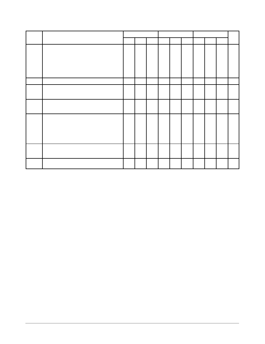
Symbol
Characteristic
40°C
25°C
85°C
Unit
Min
Typ
Max
Min
Typ
Max
Min
Typ
Max
VOUTPP Output Voltage Amplitude (@ Vinppmin)
VCC = 2.375 V to 2.625 V
fin ≤ 3 GHz
fin ≤ 5.5 GHz
VCC = 3.135 V to 3.465 V
fin ≤ 3 GHz
fin ≤ 5.5 GHz
240
115
250
130
330
220
350
250
240
115
250
130
330
220
350
250
240
115
250
130
330
220
350
250
mV
fDATA
Maximum Operating Data Rate
5
6
5
6
5
6
Gb/s
tPLH,
tPHL
Differential InputtoOutput Propagation Delay
CLKQ
SELQ
200
290
240
340
280
390
200
290
240
340
280
390
200
290
240
340
280
390
ps
tSKEW
Duty Cycle Skew (Note 11)
Within Device Skew
DevicetoDevice Skew (Note 15)
2
10
15
20
80
2
10
15
20
80
2
10
15
20
80
ps
tJITTER
RMS Random Clock Jitter (Note 13)
fin = 3 GHz
fin = 5.5 GHz
PeaktoPeak Data Dependent Jitter
(Note 14)
fDATA = 3.125 Gb/s
fDATA = 5 Gb/s
fDATA = 6.125 Gb/s
0.2
6
15
0.5
15
25
0.2
6
15
0.5
15
25
0.2
6
15
0.5
15
25
ps
VINPP
Input Voltage Swing/Sensitivity
(Differential Configuration)
75
400
2500
75
400
2500
75
400
2500
mV
tr
tf
Output Rise/Fall Times @ 1 GHz
(20% 80%)
50
75
50
75
50
75
ps
NOTE: Device will meet the specifications after thermal equilibrium has been established when mounted in a test socket or printed circuit
board with maintained transverse airflow greater than 500 lfpm. Electrical parameters are guaranteed only over the declared
operating temperature range. Functional operation of the device exceeding these conditions is not implied. Device specification limit
values are applied individually under normal operating conditions and not valid simultaneously.
10.Measured by forcing VINPP(MIN) from a 50% duty cycle clock source. All loading with an external RL = 50 W to VCC. Input edge rates 40 ps
(20% 80%).
11. Duty cycle skew is measured between differential outputs using the deviations of the sum of Tpw and Tpw+ @ 1 GHz.
12.VINPP(MAX) cannot exceed VCC VEE. Input voltage swing is a singleended measurement operating in differential mode.
13.Additive RMS jitter with 50% duty cycle clock signal.
14.Additive peaktopeak data dependent jitter with input NRZ data at PRBS 2231.
15.Devicetodevice skew is measured between outputs under identical transition and conditions @ 1 GHz.
相关PDF资料 |
PDF描述 |
|---|---|
| NB7L11MMNR2 | IC CLK/DTA BUF TRNSLA 1:2 16-QFN |
| NB7L14MMNR2 | IC CLK/DTA BUF TRNSLA 1:4 16-QFN |
| NB7L14MN1G | IC CLOCK BUFFER 1:4 8GHZ 16-QFN |
| NB7L14MN1TXG | IC BUFFER 1:4 LVPECL DIFF 16QFN |
| NB7L14MNG | IC CLOCK BUFFER 1:4 8GHZ 16-QFN |
相关代理商/技术参数 |
参数描述 |
|---|---|
| NB7L111MMNR2G | 功能描述:时钟驱动器及分配 2.5V/3.3V 6.125Gb/s 1:10 Clk/Data Driver RoHS:否 制造商:Micrel 乘法/除法因子:1:4 输出类型:Differential 最大输出频率:4.2 GHz 电源电压-最大: 电源电压-最小:5 V 最大工作温度:+ 85 C 封装 / 箱体:SOIC-8 封装:Reel |
| NB7L11M | 制造商:ONSEMI 制造商全称:ON Semiconductor 功能描述:2.5V/3.3V Differential 1:2 Clock/Data Fanout Buffer/ Translator with CML Outputs and Internal Termination |
| NB7L11MMN | 功能描述:时钟缓冲器 2.5V/3.3V Multilevel RoHS:否 制造商:Texas Instruments 输出端数量:5 最大输入频率:40 MHz 传播延迟(最大值): 电源电压-最大:3.45 V 电源电压-最小:2.375 V 最大功率耗散: 最大工作温度:+ 85 C 最小工作温度:- 40 C 封装 / 箱体:LLP-24 封装:Reel |
| NB7L11MMNEVB | 功能描述:BOARD EVAL BBG NB7L11MMN RoHS:是 类别:编程器,开发系统 >> 评估演示板和套件 系列:* 标准包装:1 系列:PCI Express® (PCIe) 主要目的:接口,收发器,PCI Express 嵌入式:- 已用 IC / 零件:DS80PCI800 主要属性:- 次要属性:- 已供物品:板 |
| NB7L11MMNG | 功能描述:时钟缓冲器 2.5V/3.3V Multilevel 1:2 Clock / Fanout RoHS:否 制造商:Texas Instruments 输出端数量:5 最大输入频率:40 MHz 传播延迟(最大值): 电源电压-最大:3.45 V 电源电压-最小:2.375 V 最大功率耗散: 最大工作温度:+ 85 C 最小工作温度:- 40 C 封装 / 箱体:LLP-24 封装:Reel |
发布紧急采购,3分钟左右您将得到回复。