- 您现在的位置:买卖IC网 > PDF目录11168 > NB7L72MMNTXG (ON Semiconductor)IC CROSSPOINT SWITCH 2X2 16QFN PDF资料下载
参数资料
| 型号: | NB7L72MMNTXG |
| 厂商: | ON Semiconductor |
| 文件页数: | 1/8页 |
| 文件大小: | 0K |
| 描述: | IC CROSSPOINT SWITCH 2X2 16QFN |
| 标准包装: | 3,000 |
| 功能: | 交叉点开关 |
| 电路: | 1 x 2:2 |
| 电压电源: | 单电源 |
| 电压 - 电源,单路/双路(±): | 2.3 V ~ 3.6 V |
| 电流 - 电源: | 135mA |
| 工作温度: | -40°C ~ 85°C |
| 安装类型: | 表面贴装 |
| 封装/外壳: | 16-VFQFN 裸露焊盘 |
| 供应商设备封装: | 16-QFN(3x3) |
| 包装: | 带卷 (TR) |
Semiconductor Components Industries, LLC, 2012
April, 2013 Rev. 3
1
Publication Order Number:
NB7L72M/D
NB7L72M
2.5V / 3.3V Differential 2 x 2
Crosspoint Switch with
CML Outputs Clock/Data
Buffer/Translator
MultiLevel Inputs w/ Internal Termination
Description
The NB7L72M is a high bandwidth, low voltage, fully differential
2 x 2 crosspoint switch with CML outputs. The NB7L72M design is
optimized for low skew and minimal jitter as it produces two identical
copies of Clock or Data operating up to 7 GHz or 10 Gb/s,
respectively. As such, the NB7L72M is ideal for SONET, GigE, Fiber
Channel, Backplane and other clock/data distribution applications.
The differential IN/IN inputs incorporate internal 50
W termination
resistors and will accept LVPECL, CML, or LVDS logic levels (see
Figure 11). The 16 mA differential CML outputs provide matching
internal 50
W terminations and produce 400 mV output swings when
externally terminated with a 50
W resistor to VCC (see Figure 9).
The NB7L72M is the 2.5 V/3.3 V version of the and NB7V72M and
is offered in a low profile 3x3 mm 16pin QFN package. Application
notes, models, and support documentation are available at
www.onsemi.com.
The NB7L72M is a member of the GigaComm
family of high
performance clock products.
Features
Maximum Input Data Rate > 10 Gb/s
Data Dependent Jitter < 10 ps pkpk
Maximum Input Clock Frequency > 7 GHz
Random Clock Jitter < 0.5 ps RMS, Max
150 ps Typical Propagation Delay
30 ps Typical Rise and Fall Times
Differential CML Outputs, 400 mV peaktopeak, typical
Operating Range: VCC = 2.375 V to 3.6 V with GND = 0 V
Internal 50 W Input Termination Resistors
QFN16 Package, 3mm x 3mm
40°C to +85°C Ambient Operating Temperature
These are PbFree Devices
A
= Assembly Location
L
= Wafer Lot
Y
= Year
W
= Work Week
G
= PbFree Package
(Note: Microdot may be in either location)
*For additional marking information, refer to
Application Note AND8002/D.
MARKING
DIAGRAM*
QFN16
MN SUFFIX
CASE 485G
http://onsemi.com
See detailed ordering and shipping information in the package
dimensions section on page 7 of this data sheet.
ORDERING INFORMATION
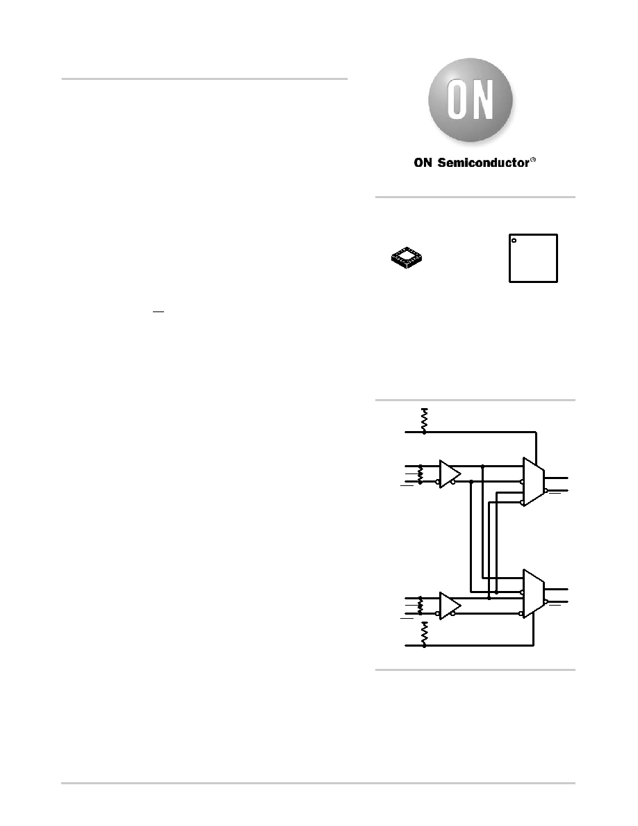
IN0
SEL0
SEL1
IN0
+
VT0
IN1
VT1
Q0
Q1
0
1
0
1
Figure 1. Logic Diagram
1
NB7L
72M
ALYWG
G
相关PDF资料 |
PDF描述 |
|---|---|
| HI4P0509-5Z | IC MULTIPLEXER DUAL 4X1 20PLCC |
| HI9P0508-9Z | IC MULTIPLEXER 8X1 16SOIC |
| R5F100JEAFA#X0 | MCU 16BIT 64KB FLASH 52LQFP |
| NB6L72MMNR2G | IC CROSSPOINT SWITCH 2X2 16QFN |
| VI-B1X-CU-B1 | CONVERTER MOD DC/DC 5.2V 200W |
相关代理商/技术参数 |
参数描述 |
|---|---|
| NB7L86M | 制造商:ONSEMI 制造商全称:ON Semiconductor 功能描述:2.5V/3.3V 12 Gb/s Differential Clock/Data SmartGate with CML Output and Internal Termination |
| NB7L86MMN | 功能描述:逻辑门 2.5V/3.3V Diff Clock RoHS:否 制造商:Texas Instruments 产品:OR 逻辑系列:LVC 栅极数量:2 线路数量(输入/输出):2 / 1 高电平输出电流:- 16 mA 低电平输出电流:16 mA 传播延迟时间:3.8 ns 电源电压-最大:5.5 V 电源电压-最小:1.65 V 最大工作温度:+ 125 C 安装风格:SMD/SMT 封装 / 箱体:DCU-8 封装:Reel |
| NB7L86MMNEVB | 功能描述:BOARD EVAL BBG NB7L86MMN RoHS:是 类别:编程器,开发系统 >> 评估演示板和套件 系列:* 标准包装:1 系列:PCI Express® (PCIe) 主要目的:接口,收发器,PCI Express 嵌入式:- 已用 IC / 零件:DS80PCI800 主要属性:- 次要属性:- 已供物品:板 |
| NB7L86MMNG | 功能描述:逻辑门 2.5V/3.3V Diff Clock Data Smart Gate RoHS:否 制造商:Texas Instruments 产品:OR 逻辑系列:LVC 栅极数量:2 线路数量(输入/输出):2 / 1 高电平输出电流:- 16 mA 低电平输出电流:16 mA 传播延迟时间:3.8 ns 电源电压-最大:5.5 V 电源电压-最小:1.65 V 最大工作温度:+ 125 C 安装风格:SMD/SMT 封装 / 箱体:DCU-8 封装:Reel |
| NB7L86MMNR2 | 功能描述:逻辑门 2.5V/3.3V Diff Clock RoHS:否 制造商:Texas Instruments 产品:OR 逻辑系列:LVC 栅极数量:2 线路数量(输入/输出):2 / 1 高电平输出电流:- 16 mA 低电平输出电流:16 mA 传播延迟时间:3.8 ns 电源电压-最大:5.5 V 电源电压-最小:1.65 V 最大工作温度:+ 125 C 安装风格:SMD/SMT 封装 / 箱体:DCU-8 封装:Reel |
发布紧急采购,3分钟左右您将得到回复。