参数资料
| 型号: | NB7L86MMNG |
| 厂商: | ON Semiconductor |
| 文件页数: | 1/12页 |
| 文件大小: | 0K |
| 描述: | IC GATE MULTI FUNCT DIFF 16-QFN |
| 标准包装: | 123 |
| 逻辑类型: | 可配置多功能 |
| 电路数: | 2 |
| 输入数: | 2 |
| 施密特触发器输入: | 无 |
| 输出类型: | 差分 |
| 电源电压: | 2.4 V ~ 3.5 V |
| 工作温度: | -40°C ~ 85°C |
| 安装类型: | 表面贴装 |
| 封装/外壳: | 16-VFQFN 裸露焊盘 |
| 供应商设备封装: | 16-QFN(3x3) |
| 包装: | 管件 |
| 其它名称: | NB7L86MMNG-ND NB7L86MMNGOS |
Semiconductor Components Industries, LLC, 2012
March, 2012 Rev. 7
1
Publication Order Number:
NB7L86M/D
NB7L86M
2.5V/3.3V 12 Gb/s Differential
Clock/Data SmartGate with
CML Output and Internal
Termination
The NB7L86M is a multifunction differential Logic Gate, which
can be configured as an AND/NAND, OR/NOR, XOR/XNOR, or 2:1
MUX. This device is part of the GigaComm family of high
performance Silicon Germanium products. The NB7L86M is an
ultralow jitter multilogic gate with a maximum data rate of 12 Gb/s
and input clock frequency of 8 GHz suitable for Data Communication
Systems, Telecom Systems, Fiber Channel, and GigE applications.
Differential inputs incorporate internal 50
W termination resistors
and accept LVNECL (Negative ECL), LVPECL (Positive ECL),
LVCMOS, LVTTL, CML, or LVDS. The differential 16 mA CML
output provides matching internal 50
W termination, and 400 mV
output swing when externally terminated 50
W to VCC.
The device is housed in a low profile 3x3 mm 16pin QFN package.
Application notes, models, and support documentation are available
on www.onsemi.com.
Features
Maximum Input Clock Frequency up to 8 GHz
Maximum Input Data Rate up to 12 Gb/s Typical
< 0.5 ps of RMS Clock Jitter
< 10 ps of Data Dependent Jitter
30 ps Typical Rise and Fall Times
90 ps Typical Propagation Delay
2 ps Typical Within Device Skew
Operating Range: VCC = 2.375 V to 3.465 V with VEE = 0 V
CML Output Level (400 mV PeaktoPeak Output) Differential Output
50 W Internal Input and Output Termination Resistors
Functionally Compatible with Existing 2.5 V/3.3 V LVEL, LVEP, EP
and SG Devices
These are PbFree Devices
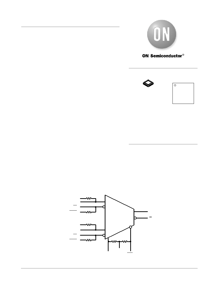
Figure 1. Simplified Logic Diagram
D0
Q
SEL
VTD0
Q
SEL
VTD0
50 W
D0
D1
VTD1
50 W
D1
50 W
VTSEL
http://onsemi.com
QFN16
MN SUFFIX
CASE 485G
MARKING
DIAGRAM*
*For additional marking information, refer to
Application Note AND8002/D.
A
= Assembly Location
L
= Wafer Lot
Y
= Year
W
= Work Week
G
= PbFree Package
16
NB7L
86M
ALYWG
G
1
See detailed ordering and shipping information in the package
dimensions section on page 11 of this data sheet.
ORDERING INFORMATION
1
相关PDF资料 |
PDF描述 |
|---|---|
| UTS612DCG | CONN PLUG SEALING CAP SIZE 12 |
| MC100EP08DTG | IC GATE XOR/XNOR ECL 2INP 8TSSOP |
| MC10EL05DTG | IC GATE AND/NAND ECL 2INP 8TSSOP |
| MC10EL04DG | IC GATE AND/NAND ECL 2INP 8SOIC |
| MC100EL04DG | IC GATE AND/NAND ECL 2INP 8SOIC |
相关代理商/技术参数 |
参数描述 |
|---|---|
| NB7L86MMNR2 | 功能描述:逻辑门 2.5V/3.3V Diff Clock RoHS:否 制造商:Texas Instruments 产品:OR 逻辑系列:LVC 栅极数量:2 线路数量(输入/输出):2 / 1 高电平输出电流:- 16 mA 低电平输出电流:16 mA 传播延迟时间:3.8 ns 电源电压-最大:5.5 V 电源电压-最小:1.65 V 最大工作温度:+ 125 C 安装风格:SMD/SMT 封装 / 箱体:DCU-8 封装:Reel |
| NB7L86MMNR2G | 功能描述:逻辑门 2.5V/3.3V Diff Clock Data Smart Gate RoHS:否 制造商:Texas Instruments 产品:OR 逻辑系列:LVC 栅极数量:2 线路数量(输入/输出):2 / 1 高电平输出电流:- 16 mA 低电平输出电流:16 mA 传播延迟时间:3.8 ns 电源电压-最大:5.5 V 电源电压-最小:1.65 V 最大工作温度:+ 125 C 安装风格:SMD/SMT 封装 / 箱体:DCU-8 封装:Reel |
| NB7LQ572 | 制造商:ONSEMI 制造商全称:ON Semiconductor 功能描述:2.5V / 3.3V Differential 4:1 Mux w/Input Equalizer to 1:2 LVPECL Clock/Data Fanout / Translator |
| NB7LQ572MNG | 功能描述:时钟缓冲器 7 GHz160 ps3.6V 3V RoHS:否 制造商:Texas Instruments 输出端数量:5 最大输入频率:40 MHz 传播延迟(最大值): 电源电压-最大:3.45 V 电源电压-最小:2.375 V 最大功率耗散: 最大工作温度:+ 85 C 最小工作温度:- 40 C 封装 / 箱体:LLP-24 封装:Reel |
| NB7LQ572MNR4G | 功能描述:时钟缓冲器 7 GHz160 ps3.6V 3V RoHS:否 制造商:Texas Instruments 输出端数量:5 最大输入频率:40 MHz 传播延迟(最大值): 电源电压-最大:3.45 V 电源电压-最小:2.375 V 最大功率耗散: 最大工作温度:+ 85 C 最小工作温度:- 40 C 封装 / 箱体:LLP-24 封装:Reel |
发布紧急采购,3分钟左右您将得到回复。