参数资料
| 型号: | NBSG14MNHTBG |
| 厂商: | ON Semiconductor |
| 文件页数: | 12/13页 |
| 文件大小: | 0K |
| 描述: | IC CLK/DATA BUFF 1:4 12GHZ 16QFN |
| 标准包装: | 100 |
| 类型: | 扇出缓冲器(分配),数据 |
| 电路数: | 1 |
| 比率 - 输入:输出: | 1:4 |
| 差分 - 输入:输出: | 是/是 |
| 输入: | CML,LVCMOS,LVDS,LVTTL,NECL,PECL,RSECL |
| 输出: | RSECL,RSNECL,RSPECL |
| 频率 - 最大: | 12GHz |
| 电源电压: | 2.375 V ~ 3.465 V |
| 工作温度: | -40°C ~ 85°C |
| 安装类型: | 表面贴装 |
| 封装/外壳: | 16-VFQFN 裸露焊盘 |
| 供应商设备封装: | 16-QFN(3x3) |
| 包装: | 带卷 (TR) |
NBSG14
http://onsemi.com
8
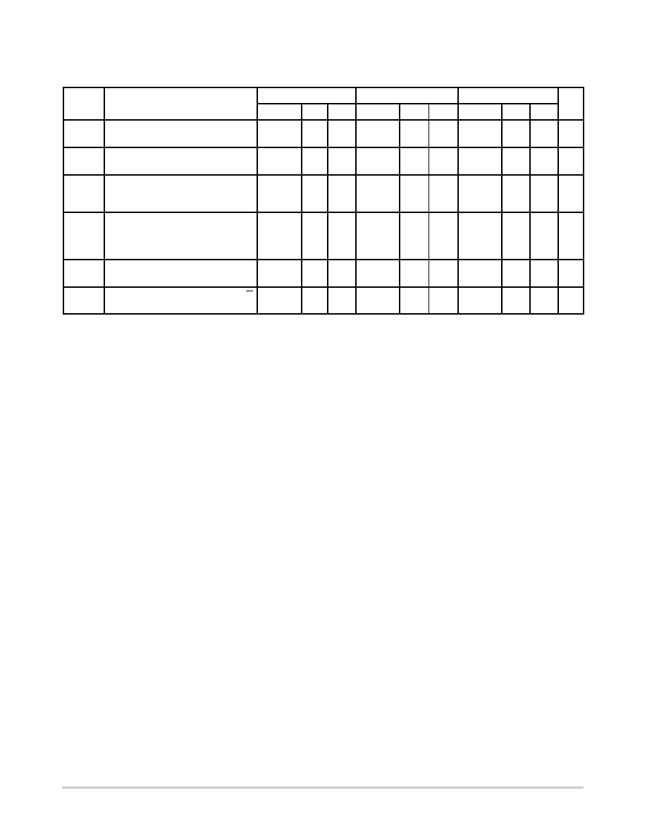
Table 8. AC CHARACTERISTICS for FCBGA16
VCC = 0 V; VEE = 3.465 V to 2.375 V or VCC = 2.375 V to 3.465 V; VEE = 0 V
Symbol
Characteristic
40°C
25°C
70°C
Unit
Min
Typ
Max
Min
Typ
Max
Min
Typ
Max
fmax
Maximum Frequency
10.7
12
10.7
12
10.7
12
GHz
tPLH,
tPHL
Propagation Delay to
Output Differential
100
125
150
100
125
150
100
125
150
ps
tSKEW
Duty Cycle Skew (Note 23)
WithinDevice Skew (Note 24)
DevicetoDevice Skew (Note 25)
2
6
25
10
15
50
2
6
25
10
15
50
2
6
25
10
15
50
ps
tJITTER
RMS Random Clock Jitter
fin < 10 GHz
PeaktoPeak Data Dependent Jitter
(Note 28)
fin < 10 Gb/s
0.2
10
1
0.2
10
1
0.2
10
1
ps
VINPP
Input Voltage Swing/Sensitivity
(Differential Configuration) (Note 26)
75
2600
75
2600
75
2600
mV
tr
tf
Output Rise/Fall Times
Q, Q
(20% 80%) @ 1 GHz
20
30
55
20
30
55
20
30
55
ps
NOTE: Device will meet the specifications after thermal equilibrium has been established when mounted in a test socket or printed circuit
board with maintained transverse airflow greater than 500 lfpm. Electrical parameters are guaranteed only over the declared
operating temperature range. Functional operation of the device exceeding these conditions is not implied. Device specification limit
values are applied individually under normal operating conditions and not valid simultaneously.
22.Measured using a 500 mV source, 50% duty cycle clock source. All outputs loaded with 50 W to VCC 1.5 V. Input edge rates 40 ps
(20% 80%).
24.WithinDevice skew is measured between outputs under identical transitions and conditions on any one device.
25.Devicetodevice skew for identical transitions at identical VCC levels.
26.VINPP (MAX) cannot exceed VCC VEE (applicable only when VCCVEE < 2600 mV).
27.Additive RMS Jitter with 50% duty cycle clock signal at 10 GHz.
28.Additive PeaktoPeak data dependent jitter with NRZ PRBS 2311 data at 10 Gb/s.
相关PDF资料 |
PDF描述 |
|---|---|
| NB7L111MMNR2G | IC CLK/DATA BUFF MUX 2:10 52-QFN |
| AD5412AREZ-REEL7 | IC DAC 12BIT SER 24-TSSOP |
| V300A24H500BF2 | CONVERTER MOD DC/DC 24V 500W |
| V300A24H500BF | CONVERTER MOD DC/DC 24V 500W |
| VE-JT4-MY | CONVERTER MOD DC/DC 48V 50W |
相关代理商/技术参数 |
参数描述 |
|---|---|
| NBSG14MNR2 | 功能描述:时钟缓冲器 2.5V/3.3V SiGE 1:4 RoHS:否 制造商:Texas Instruments 输出端数量:5 最大输入频率:40 MHz 传播延迟(最大值): 电源电压-最大:3.45 V 电源电压-最小:2.375 V 最大功率耗散: 最大工作温度:+ 85 C 最小工作温度:- 40 C 封装 / 箱体:LLP-24 封装:Reel |
| NBSG14MNR2G | 功能描述:时钟缓冲器 2.5V/3.3V SiGE 1:4 Diff Clock w/RSECL RoHS:否 制造商:Texas Instruments 输出端数量:5 最大输入频率:40 MHz 传播延迟(最大值): 电源电压-最大:3.45 V 电源电压-最小:2.375 V 最大功率耗散: 最大工作温度:+ 85 C 最小工作温度:- 40 C 封装 / 箱体:LLP-24 封装:Reel |
| NBSG16 | 制造商:ONSEMI 制造商全称:ON Semiconductor 功能描述:2.5V/3.3V SiGe Differential Receiver/Driver with RSECLOutputs |
| NBSG16/D | 制造商:未知厂家 制造商全称:未知厂家 功能描述:2.5V/3.3V SiGe Differential Receiver/Driver with RSECL Outputs |
| NBSG16BA | 功能描述:缓冲器和线路驱动器 2.5V/3.3V SiGe Diff RoHS:否 制造商:Micrel 输入线路数量:1 输出线路数量:2 极性:Non-Inverting 电源电压-最大:+/- 5.5 V 电源电压-最小:+/- 2.37 V 最大工作温度:+ 85 C 安装风格:SMD/SMT 封装 / 箱体:MSOP-8 封装:Reel |
发布紧急采购,3分钟左右您将得到回复。