参数资料
| 型号: | NBSG14MNR2 |
| 厂商: | ON Semiconductor |
| 文件页数: | 6/13页 |
| 文件大小: | 0K |
| 描述: | IC CLK/DATA BUFF 1:4 12GHZ 16QFN |
| 产品变化通告: | LTB Notification 06/Feb/2008 |
| 标准包装: | 1 |
| 类型: | 扇出缓冲器(分配),数据 |
| 电路数: | 1 |
| 比率 - 输入:输出: | 1:4 |
| 差分 - 输入:输出: | 是/是 |
| 输入: | CML,LVCMOS,LVDS,LVTTL,NECL,PECL,RSECL |
| 输出: | RSECL,RSNECL,RSPECL |
| 频率 - 最大: | 12GHz |
| 电源电压: | 2.375 V ~ 3.465 V |
| 工作温度: | -40°C ~ 85°C |
| 安装类型: | 表面贴装 |
| 封装/外壳: | 16-VFQFN 裸露焊盘 |
| 供应商设备封装: | 16-QFN(3x3) |
| 包装: | 标准包装 |
| 其它名称: | NBSG14MNR2OSDKR |
NBSG14
http://onsemi.com
2
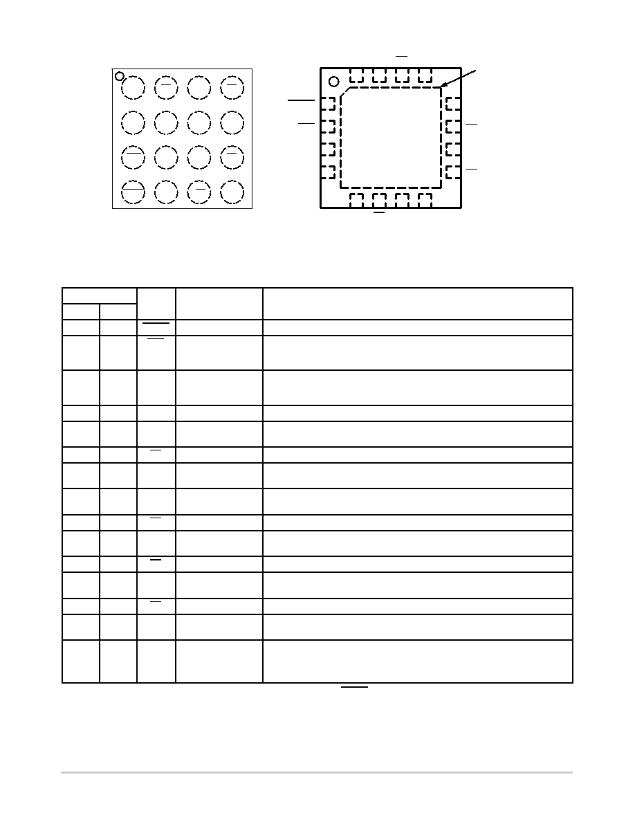
Figure 1. BGA16 Pinout (Top View)
VTCLK
CLK
VEE
VTCLK
Q0
VEE
Q3
Q2
VCC
Q0
Q1
Q2
A
B
C
D
12
3
4
VEE Q3
Q3 VCC
VEE Q0
Q0
VCC
Q1
Q2
VTCLK
CLK
VTCLK
56
7
8
16
15
14
13
12
11
10
9
1
2
3
4
NBSG14
Exposed Pad (EP)
Figure 2. QFN16 Pinout (Top View)
Table 1. Pin Description
Pin
Name
I/O
Description
BGA
QFN
D1
1
VTCLK
Internal 50 W Termination pin. See Table 2.
C1
2
CLK
ECL, CML,
LVCMOS, LVDS,
LVTTL Input
Inverted Differential Input. Internal 75 kW to VEE and 36.5 kW to VCC.
B1
3
CLK
ECL, CML,
LVCMOS, LVDS,
LVTTL Input
Noninverted Differential Input. Internal 75 kW to VEE.
A1
4
VTCLK
Internal 50 W Termination Pin. See Table 2.
B2,C2
5,16
VEE
Negative Supply Voltage. All VEE Pins must be Externally Connected to Power
Supply to Guarantee Proper Operation.
A2*
6
Q3
RSECL Output
Inverted Differential Output 3. Typically Terminated with 50 W to VTT = VCC 2 V*
A3*
7
Q3
RSECL Output
Noninverted Differential Output 3. Typically Terminated with 50 W to
VTT = VCC 2 V*
B3,C3
8,13
VCC
Positive Supply Voltage. All VCC Pins must be Externally Connected to Power
Supply to Guarantee Proper Operation.
A4*
9
Q2
RSECL Output
Inverted Differential Output 2. Typically Terminated with 50 W to VTT = VCC 2 V*
B4*
10
Q2
RSECL Output
Noninverted Differential Output 2. Typically Terminated with 50 W to
VTT = VCC 2 V*
C4*
11
Q1
RSECL Output
Inverted Differential Output 1. Typically Terminated with 50 W to VTT = VCC 2 V*
D4*
12
Q1
RSECL Output
Noninverted Differential Output 1. Typically Terminated with 50 W to
VTT = VCC 2 V*
D3*
14
Q0
RSECL Output
Inverted Differential Output 0. Typically Terminated with 50 W to VTT = VCC 2 V*
D2*
15
Q0
RSECL Output
Noninverted Differential Output 0. Typically Terminated with 50 W to
VTT = VCC 2 V*
N/A
EP
The Exposed Pad (EP) and the QFN16 package bottom is thermally connected
to the die for improved heat transfer out of package. The exposed pad must be
attached to a heatsinking conduit. The pad is not electrically connected to the die
but may be electrically and thermally connected to VEE on the PC board.
1. In the differential configuration when the input termination pins (VTCLK, VTCLK) are connected to a common termination voltage, if no
signal is applied then the device will be susceptible to selfoscillation.
*Devices in BGA package typically terminated with 50 W to VTT = VCC 1.5 V.
相关PDF资料 |
PDF描述 |
|---|---|
| AD7305BR | IC DAC 8BIT QUAD 5V R-R 20-SOIC |
| AD7533KR | IC DAC 10BIT MULTIPLYING 16-SOIC |
| AD7945BN | IC DAC 12BIT MULT PARALL 20-DIP |
| AD7943BN | IC DAC 12BIT MULT SRL 16-DIP |
| AD7804BRZ-REEL | IC DAC 10BIT QUAD SRL 16-SOIC |
相关代理商/技术参数 |
参数描述 |
|---|---|
| NBSG14MNR2G | 功能描述:时钟缓冲器 2.5V/3.3V SiGE 1:4 Diff Clock w/RSECL RoHS:否 制造商:Texas Instruments 输出端数量:5 最大输入频率:40 MHz 传播延迟(最大值): 电源电压-最大:3.45 V 电源电压-最小:2.375 V 最大功率耗散: 最大工作温度:+ 85 C 最小工作温度:- 40 C 封装 / 箱体:LLP-24 封装:Reel |
| NBSG16 | 制造商:ONSEMI 制造商全称:ON Semiconductor 功能描述:2.5V/3.3V SiGe Differential Receiver/Driver with RSECLOutputs |
| NBSG16/D | 制造商:未知厂家 制造商全称:未知厂家 功能描述:2.5V/3.3V SiGe Differential Receiver/Driver with RSECL Outputs |
| NBSG16BA | 功能描述:缓冲器和线路驱动器 2.5V/3.3V SiGe Diff RoHS:否 制造商:Micrel 输入线路数量:1 输出线路数量:2 极性:Non-Inverting 电源电压-最大:+/- 5.5 V 电源电压-最小:+/- 2.37 V 最大工作温度:+ 85 C 安装风格:SMD/SMT 封装 / 箱体:MSOP-8 封装:Reel |
| NBSG16BAEVB | 功能描述:BOARD EVALUATION BBG NBSG16BA RoHS:否 类别:编程器,开发系统 >> 过时/停产零件编号 系列:- 标准包装:1 系列:- 传感器类型:CMOS 成像,彩色(RGB) 传感范围:WVGA 接口:I²C 灵敏度:60 fps 电源电压:5.7 V ~ 6.3 V 嵌入式:否 已供物品:成像器板 已用 IC / 零件:KAC-00401 相关产品:4H2099-ND - SENSOR IMAGE WVGA COLOR 48-PQFP4H2094-ND - SENSOR IMAGE WVGA MONO 48-PQFP |
发布紧急采购,3分钟左右您将得到回复。