参数资料
| 型号: | NBSG16MMN |
| 厂商: | ON Semiconductor |
| 文件页数: | 10/11页 |
| 文件大小: | 0K |
| 描述: | IC RCVR/DRVR CML 2.5V/3.3V 16QFN |
| 产品变化通告: | LTB Notification 06/Feb/2008 |
| 标准包装: | 123 |
| 类型: | 收发器 |
| 应用: | 仪表 |
| 安装类型: | 表面贴装 |
| 封装/外壳: | 16-VFQFN 裸露焊盘 |
| 供应商设备封装: | 16-QFN(3x3) |
| 包装: | 管件 |
| 其它名称: | NBSG16MMNOS |
NBSG16M
http://onsemi.com
8
Table 8. AC CHARACTERISTICS VCC = 0 V; VEE = 3.465 V to 2.375 V or VCC = 2.375 V to 3.465 V; VEE = 0 V
Symbol
Characteristic
40°C
25°C
85°C
Unit
Min
Typ
Max
Min
Typ
Max
Min
Typ
Max
VOUTPP Output Voltage Amplitude
fin < 7 GHz
fin < 10 GHz
300
200
400
250
300
200
400
250
300
100
400
150
mV
tPLH,
tPHL
Propagation Delay to
Output Differential
90
110
150
100
120
150
100
125
155
ps
tSKEW
Duty Cycle Skew (Note 16)
3
15
3
15
3
15
ps
tJITTER
RMS Random Clock Jitter (Note 18)
fin < 10 GHz
PeaktoPeak Data Dependent Jitter (Note 19)
fin < 10 Gb/s
0.2
8
1
15
0.2
8
1
15
0.2
8
1.0
15
ps
VINPP
Input Voltage Swing/Sensitivity
(Differential Configuration) (Note 17)
75
2500
75
2500
75
2500
mV
tr
tf
Output Rise/Fall Times @ 1 GHz
Q, Q
(20% 80%)
21
35
53
21
35
53
21
35
53
ps
NOTE: Device will meet the specifications after thermal equilibrium has been established when mounted in a test socket or printed circuit
board with maintained transverse airflow greater than 500 lfpm. Electrical parameters are guaranteed only over the declared
operating temperature range. Functional operation of the device exceeding these conditions is not implied. Device specification
limit values are applied individually under normal operating conditions and not valid simultaneously.
15.Measured using a 400 mV source, 50% duty cycle clock source. All loading with 50 W to VCC. Input edge rates 40 ps (20% 80%).
17.VINPP(max) cannot exceed VCC VEE. (Applicable only when VCC VEE < 2500 mV). Input voltage swing is a singleended measurement
operating in differential mode.
18.Additive RMS jitter with 50% duty cycle clock signal at 10GHz.
19.Additive PeaktoPeak data dependent jitter with NRZ PRBS2311 data rate at 10 Gb/s.
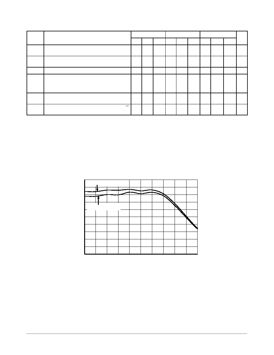
Figure 4. Output Voltage Amplitude (VOUTPP) versus
Input Clock Frequency (fin) at Ambient Temperature (Typical)
0
50
100
150
200
250
300
350
400
450
500
01
23456
789
10
FREQUENCY (GHz)
OUTPUT
VOL
TAGE
AMPLITUDE
(mV)
VCC VEE = 3.3 V
VCC VEE = 2.5 V
相关PDF资料 |
PDF描述 |
|---|---|
| NBSG16BA | IC RCVR/DRVR RSECL SIGE 16FCBGA |
| EMC43DRAS-S734 | CONN EDGECARD 86POS .100 R/A PCB |
| GSC65DRTN-S13 | CONN EDGECARD 130PS .100 EXTEND |
| GMC65DRTN-S13 | CONN EDGECARD 130POS .100 EXTEND |
| GSC65DRTH-S13 | CONN EDGECARD 130PS .100 EXTEND |
相关代理商/技术参数 |
参数描述 |
|---|---|
| NBSG16MMNEVB | 功能描述:BOARD EVALUATION BBG NBSG16MMN RoHS:否 类别:编程器,开发系统 >> 过时/停产零件编号 系列:- 标准包装:1 系列:- 传感器类型:CMOS 成像,彩色(RGB) 传感范围:WVGA 接口:I²C 灵敏度:60 fps 电源电压:5.7 V ~ 6.3 V 嵌入式:否 已供物品:成像器板 已用 IC / 零件:KAC-00401 相关产品:4H2099-ND - SENSOR IMAGE WVGA COLOR 48-PQFP4H2094-ND - SENSOR IMAGE WVGA MONO 48-PQFP |
| NBSG16MMNG | 功能描述:缓冲器和线路驱动器 2.5V/3.3V Multilevel Input Clk/Data RCVR RoHS:否 制造商:Micrel 输入线路数量:1 输出线路数量:2 极性:Non-Inverting 电源电压-最大:+/- 5.5 V 电源电压-最小:+/- 2.37 V 最大工作温度:+ 85 C 安装风格:SMD/SMT 封装 / 箱体:MSOP-8 封装:Reel |
| NBSG16MMNR2 | 功能描述:缓冲器和线路驱动器 2.5V/3.3V Multilevel RoHS:否 制造商:Micrel 输入线路数量:1 输出线路数量:2 极性:Non-Inverting 电源电压-最大:+/- 5.5 V 电源电压-最小:+/- 2.37 V 最大工作温度:+ 85 C 安装风格:SMD/SMT 封装 / 箱体:MSOP-8 封装:Reel |
| NBSG16MMNR2G | 功能描述:缓冲器和线路驱动器 2.5V/3.3V Multilevel Input Clk/Data RCVR RoHS:否 制造商:Micrel 输入线路数量:1 输出线路数量:2 极性:Non-Inverting 电源电压-最大:+/- 5.5 V 电源电压-最小:+/- 2.37 V 最大工作温度:+ 85 C 安装风格:SMD/SMT 封装 / 箱体:MSOP-8 封装:Reel |
| NBSG16MN | 功能描述:缓冲器和线路驱动器 2.5V/3.3V SiGe Diff RoHS:否 制造商:Micrel 输入线路数量:1 输出线路数量:2 极性:Non-Inverting 电源电压-最大:+/- 5.5 V 电源电压-最小:+/- 2.37 V 最大工作温度:+ 85 C 安装风格:SMD/SMT 封装 / 箱体:MSOP-8 封装:Reel |
发布紧急采购,3分钟左右您将得到回复。