参数资料
| 型号: | NBSG16VSMAG |
| 厂商: | ON Semiconductor |
| 文件页数: | 13/14页 |
| 文件大小: | 0K |
| 描述: | IC RCVR/DRVR SIGE DIFF 16-FCLGA |
| 产品变化通告: | Product Discontinuation 04/April/2008 |
| 标准包装: | 92 |
| 类型: | 收发器 |
| 应用: | 仪表 |
| 安装类型: | 表面贴装 |
| 封装/外壳: | 16-VFQFN 裸露焊盘 |
| 供应商设备封装: | 16-QFN(3x3) |
| 包装: | 管件 |
NBSG16VS
http://onsemi.com
8
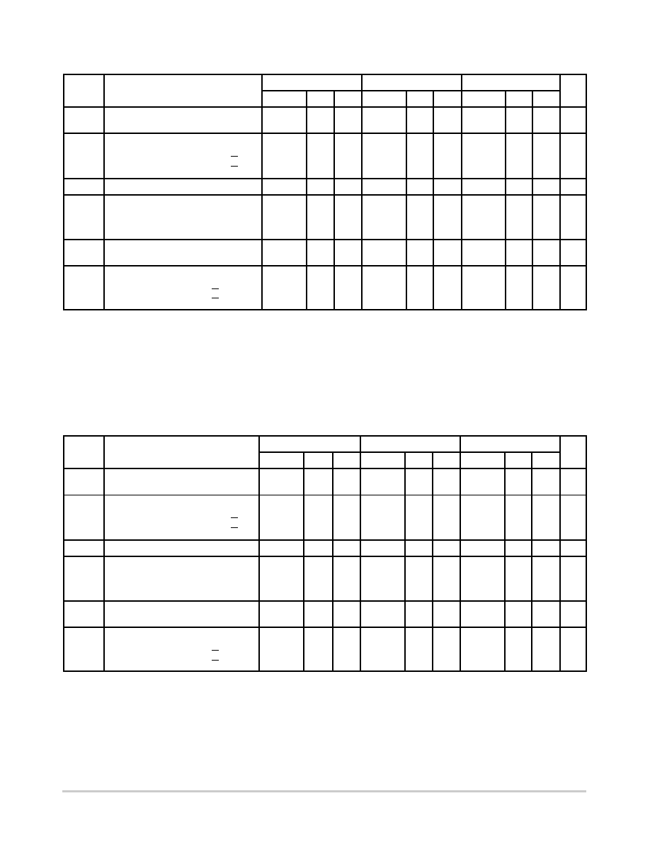
Table 8. AC CHARACTERISTICS for FCBGA16 VCC = 0 V; VEE = 3.465 V to 3.0 V or VCC = 3.0 V to 3.465 V; VEE = 0 V
Symbol
Characteristic
40°C
25°C
85°C
Unit
Min
Typ
Max
Min
Typ
Max
Min
Typ
Max
fmax
Maximum Frequency
10.7
(Note 29)
12
10.7
(Note 29)
12
10.7
(Note 29)
12
GHz
tPLH,
tPHL
Propagation Delay to Output Differen-
tial
(VCTRL = VCC 2 V) D → Q, Q
(VCTRL = VCC 1 V) D → Q, Q
100
125
120
145
140
100
125
120
145
140
100
125
120
145
140
ps
tSKEW
Duty Cycle Skew (Note 27)
3
10
3
10
3
10
ps
tJITTER
RMS Random Clock Jitter
fin < 10 GHz
PeaktoPeak Data Dependent Jitter
fin < 10 Gb/s
0.8
TBD
2
0.8
TBD
2
0.8
TBD
2
ps
VINPP
Input Voltage Swing/Sensitivity
(Differential Configuration) (Note 28)
75
2600
75
2600
75
2600
mV
tr
tf
Output Rise/Fall Times (20% 80%)
@ 1 GHz
(VCTRL = VCC 2 V) Q, Q
(VCTRL = VCC 1 V) Q, Q
30
45
40
55
50
30
45
40
55
50
30
45
40
55
50
ps
NOTE: Device will meet the specifications after thermal equilibrium has been established when mounted in a test socket or printed circuit
board with maintained transverse airflow greater than 500 lfpm. Electrical parameters are guaranteed only over the declared
operating temperature range. Functional operation of the device exceeding these conditions is not implied. Device specification limit
values are applied individually under normal operating conditions and not valid simultaneously.
26.Measured using a 500 mV source, 50% duty cycle clock source. All loading with 50 W to VCC2.0 V. Input edge rates 40 ps (20% 80%).
28.VINPP(MAX) cannot exceed VCC VEE (applicable only when VCC VEE t 2600 mV).
29.Conditions include input amplitude of 500 mV and VCTRL = VCC 2 V. Minimum output amplitude guarantee of 100 mV (see Output PP
Spec in Figure 8).
Table 9. AC CHARACTERISTICS for FCBGA16 VCC = 0 V; 3.0 V tVEE v 2.375 V or 2.375 V v VCC t 3.0 V; VEE = 0 V
Symbol
Characteristic
40°C
25°C
85°C
Unit
Min
Typ
Max
Min
Typ
Max
Min
Typ
Max
fmax
Maximum Frequency
10.7
(Note 33)
12
10.7
(Note 33)
12
10.7
(Note 33)
12
GHz
tPLH,
tPHL
Propagation Delay to Output Differen-
tial
(VCTRL = VCC 2 V) D → Q, Q
(VCTRL = VCC 1 V) D → Q, Q
100
125
120
145
140
100
125
120
145
140
100
125
120
145
140
ps
tSKEW
Duty Cycle Skew (Note 31)
3
10
3
10
3
10
ps
tJITTER
RMS Random Clock Jitter
fin < 10 GHz
PeaktoPeak Data Dependent Jitter
fin < 10 Gb/s
0.9
TBD
3
0.9
TBD
3
0.9
TBD
3
ps
VINPP
Input Voltage Swing/Sensitivity
(Differential Configuration) (Note 32)
75
2600
75
2600
75
2600
mV
tr
tf
Output Rise/Fall Times (20% 80%)
@ 1 GHz
(VCTRL = VCC 2 V) Q, Q
(VCTRL = VCC 1 V) Q, Q
25
22
50
45
70
60
25
22
50
45
70
60
25
22
50
45
70
60
ps
NOTE: Device will meet the specifications after thermal equilibrium has been established when mounted in a test socket or printed circuit
board with maintained transverse airflow greater than 500 lfpm. Electrical parameters are guaranteed only over the declared
operating temperature range. Functional operation of the device exceeding these conditions is not implied. Device specification limit
values are applied individually under normal operating conditions and not valid simultaneously.
30.Measured using a 500 mV source, 50% duty cycle clock source. All loading with 50 W to VCC2.0 V. Input edge rates 40 ps (20% 80%).
32.VINPP(MAX) cannot exceed VCC VEE (applicable only when VCC VEE t 2600 mV).
33.Conditions include input amplitude of 500 mV and VCTRL = VCC 2 V. Minimum output amplitude guarantee of 100 mV (see Output PP
Spec in Figure 9).
相关PDF资料 |
PDF描述 |
|---|---|
| CS8190EDWF20 | IC TACH/SPEEDO DRVR PREC 20SOICW |
| MCZ79076EG | IC IGNITION CTRL ELECTR 16-SOIC |
| MC33780EGR2 | IC DBUS MASTER DUAL DIFF 16-SOIC |
| MC44BS373CAFC | IC MODULATOR AUD/VID U/V 20-QFN |
| LFX200EB-03F256C | IC FPGA 200K GATES 256-BGA |
相关代理商/技术参数 |
参数描述 |
|---|---|
| NBSG16VSMN | 功能描述:缓冲器和线路驱动器 2.5V/3.3V SiGe Diff RoHS:否 制造商:Micrel 输入线路数量:1 输出线路数量:2 极性:Non-Inverting 电源电压-最大:+/- 5.5 V 电源电压-最小:+/- 2.37 V 最大工作温度:+ 85 C 安装风格:SMD/SMT 封装 / 箱体:MSOP-8 封装:Reel |
| NBSG16VSMNG | 功能描述:缓冲器和线路驱动器 2.5V/3.3V SiGe Diff w/Variable Output RoHS:否 制造商:Micrel 输入线路数量:1 输出线路数量:2 极性:Non-Inverting 电源电压-最大:+/- 5.5 V 电源电压-最小:+/- 2.37 V 最大工作温度:+ 85 C 安装风格:SMD/SMT 封装 / 箱体:MSOP-8 封装:Reel |
| NBSG16VSMNHTBG | 功能描述:缓冲器和线路驱动器 BBG 2.5V/3.3V SIGE DIFF RoHS:否 制造商:Micrel 输入线路数量:1 输出线路数量:2 极性:Non-Inverting 电源电压-最大:+/- 5.5 V 电源电压-最小:+/- 2.37 V 最大工作温度:+ 85 C 安装风格:SMD/SMT 封装 / 箱体:MSOP-8 封装:Reel |
| NBSG16VSMNR2 | 功能描述:缓冲器和线路驱动器 2.5V/3.3V SiGe Diff RoHS:否 制造商:Micrel 输入线路数量:1 输出线路数量:2 极性:Non-Inverting 电源电压-最大:+/- 5.5 V 电源电压-最小:+/- 2.37 V 最大工作温度:+ 85 C 安装风格:SMD/SMT 封装 / 箱体:MSOP-8 封装:Reel |
| NBSG16VSMNR2G | 功能描述:缓冲器和线路驱动器 2.5V/3.3V SiGe Diff w/Variable Output RoHS:否 制造商:Micrel 输入线路数量:1 输出线路数量:2 极性:Non-Inverting 电源电压-最大:+/- 5.5 V 电源电压-最小:+/- 2.37 V 最大工作温度:+ 85 C 安装风格:SMD/SMT 封装 / 箱体:MSOP-8 封装:Reel |
发布紧急采购,3分钟左右您将得到回复。