参数资料
| 型号: | NBVSPA013LN1TAG |
| 厂商: | ON Semiconductor |
| 文件页数: | 4/7页 |
| 文件大小: | 0K |
| 描述: | IC VCXO LVDS 212MHZ 6CLCC |
| 标准包装: | 1,000 |
| 系列: | PureEdge™ |
| 类型: | VCXO |
| 频率: | 212MHz |
| 电源电压: | 2.375 V ~ 2.625 V |
| 电流 - 电源: | 75mA |
| 工作温度: | -40°C ~ 85°C |
| 封装/外壳: | * |
| 包装: | * |
| 供应商设备封装: | * |
| 安装类型: | * |
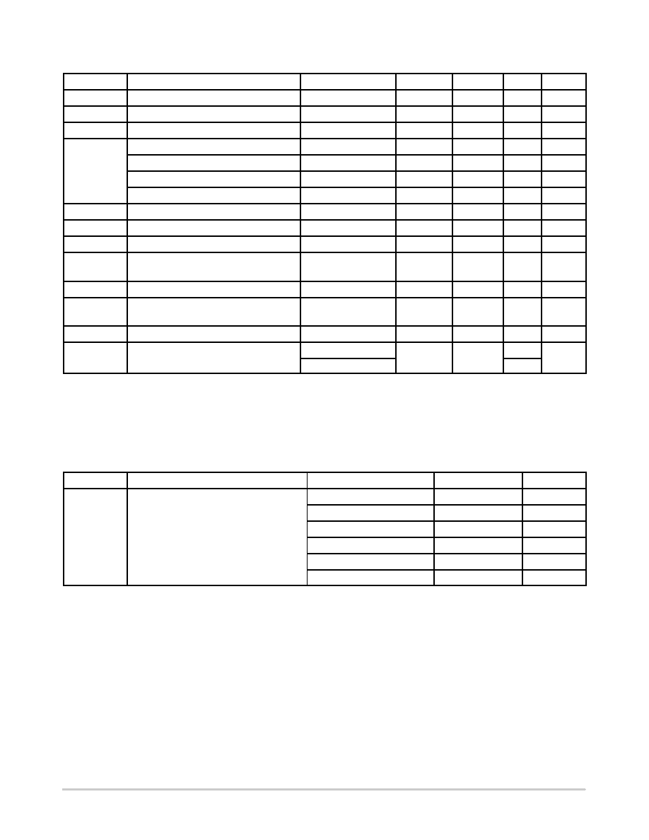
NBVSPA013
http://onsemi.com
4
Symbol
Characteristic
Conditions
Min.
Typ.
Max.
Unit
fCLKOUT
Output Clock Frequency
NBVSPA013
212.00
MHz
Df
Frequency Stability
(Note 5)
±50
ppm
tjit(f)
RMS Phase Jitter
12 kHz to 20 MHz
0.4
0.9
ps
tjitter
Cycle to Cycle, RMS
1000 Cycles
3
8
ps
Cycle to Cycle, PeaktoPeak
1000 Cycles
15
30
ps
Period, RMS
10,000 Cycles
2
4
ps
Period, PeaktoPeak
10,000 Cycles
10
20
ps
tOE/OD
Output Enable/Disable Time
200
ns
FP
Crystal Pullability (Note 6)
0 V ≤ VC ≤ VDD
±100
ppm
VC(bw)
Control Voltage Bandwidth
3 dB
20
KHz
tDUTY_CYCLE
Output Clock Duty Cycle
(Measured at Cross Point)
45
50
55
%
tR
Output Rise Time (20% and 80%)
245
400
ps
tF
Output Fall Time
(80% and 20%)
245
400
ps
tstart
Startup Time
1
5
ms
Aging
1st Year
3
ppm
Every Year After 1st
1
NOTE: Device will meet the specifications after thermal equilibrium has been established when mounted in a test socket or printed circuit
board with maintained transverse airflow greater than 500 Ifpm. Electrical parameters are guaranteed only over the declared
operating temperature range. Functional operation of the device exceeding these conditions is not implied. Device specification limit
values are applied individually under normal operating conditions and not valid simultaneously.
4. Measurement taken with outputs terminated with 100 ohm across differential pair. See Figure 4.
5. Parameter guarantees 10 years of aging. Includes initial stability at 25°C, shock, vibration and first year aging.
6. Gain transfer is positive with a rate of 130 ppm/V.
Table 7. PHASE NOISE PERFORMANCE FOR NBVSPA013
Parameter
Characteristic
Condition
212.00 MHZ
Unit
fNOISE
Output PhaseNoise Performance
100 Hz of Carrier
82
dBc/Hz
1 kHz of Carrier
110
dBc/Hz
10 kHz of Carrier
122
dBc/Hz
100 kHz of Carrier
123
dBc/Hz
1 MHz of Carrier
132
dBc/Hz
10 MHz of Carrier
160
dBc/Hz
相关PDF资料 |
PDF描述 |
|---|---|
| NBVSBA041LN1TAG | IC VCXO LVPECL 693.4830MHZ 6CLCC |
| NBVSBA037LN1TAG | IC VCXO LVPECL 707.3527MHZ 6CLCC |
| NBVSBA015LN1TAG | IC OSC VCXO 200MHZ 6CLCC |
| NBVSBA018LN1TAG | IC VCXO LVPECL 155.52MHZ 6CLCC |
| NBVSBA027LN1TAG | IC VCXO LVPECL 148.5MHZ 6CLCC |
相关代理商/技术参数 |
参数描述 |
|---|---|
| NBVSPA013LNHTAG | 功能描述:时钟发生器及支持产品 VCXO LVDS 212 MHZ RoHS:否 制造商:Silicon Labs 类型:Clock Generators 最大输入频率:14.318 MHz 最大输出频率:166 MHz 输出端数量:16 占空比 - 最大:55 % 工作电源电压:3.3 V 工作电源电流:1 mA 最大工作温度:+ 85 C 安装风格:SMD/SMT 封装 / 箱体:QFN-56 |
| NBVSPA015 | 制造商:ONSEMI 制造商全称:ON Semiconductor 功能描述:3.3 V, LVDS Voltage-Controlled Clock Oscillator (VCXO) PureEdge Product Series |
| NBVSPA015LN1TAG | 功能描述:VCXO振荡器 VCXO LVDS 200 MHZ RoHS:否 制造商:Fox 封装 / 箱体:5 mm x 3.2 mm 频率:19.2 Mhz 频率稳定性:2.5 PPM 输出格式: 封装:Reel 电源电压:3 V 端接类型:SMD/SMT 尺寸:3.2 mm W x 5 mm L x 1.5 mm H 最小工作温度:- 20 C 最大工作温度:+ 75 C |
| NBVSPA015LNHTAG | 功能描述:VCXO振荡器 VCXO LVDS 200 MHZ RoHS:否 制造商:Fox 封装 / 箱体:5 mm x 3.2 mm 频率:19.2 Mhz 频率稳定性:2.5 PPM 输出格式: 封装:Reel 电源电压:3 V 端接类型:SMD/SMT 尺寸:3.2 mm W x 5 mm L x 1.5 mm H 最小工作温度:- 20 C 最大工作温度:+ 75 C |
| NBVSPA017LN1TAG | 功能描述:VCXO振荡器 VCXO LVDS 156.25 MHZ RoHS:否 制造商:Fox 封装 / 箱体:5 mm x 3.2 mm 频率:19.2 Mhz 频率稳定性:2.5 PPM 输出格式: 封装:Reel 电源电压:3 V 端接类型:SMD/SMT 尺寸:3.2 mm W x 5 mm L x 1.5 mm H 最小工作温度:- 20 C 最大工作温度:+ 75 C |
发布紧急采购,3分钟左右您将得到回复。