参数资料
| 型号: | NBXDBA015LN1TAG |
| 厂商: | ON Semiconductor |
| 文件页数: | 4/6页 |
| 文件大小: | 0K |
| 描述: | IC CLK XO 200.0/206.9MHZ 6CLCC |
| 产品培训模块: | XO Replacement Overview |
| 标准包装: | 1 |
| 系列: | PureEdge™ |
| 类型: | 振荡器 - 晶体 |
| 频率: | 200MHz,206.9MHz |
| 电源电压: | 2.97 V ~ 3.63 V |
| 电流 - 电源: | 82mA |
| 工作温度: | -40°C ~ 85°C |
| 封装/外壳: | 6-CLCC |
| 包装: | 标准包装 |
| 供应商设备封装: | 6-CLCC(7x5) |
| 安装类型: | 表面贴装 |
| 其它名称: | NBXDBA015LN1TAGOSDKR |
NBXDBA015, NBXDBB015
http://onsemi.com
4
Symbol
Characteristic
Conditions
Min.
Typ.
Max.
Units
fCLKOUT
Output Clock Frequency
FSEL = HIGH
206.9
MHz
FSEL = LOW
200
Df
Frequency Stability NBXDBB015*
Frequency Stability NBXDBA015
0°C to +70°C
60°C to +85°C
(Note 4)
±20*
±50
ppm
FNOISE
PhaseNoise Performance
100 Hz of Carrier
102
dBc/Hz
fCLKout = 200 MHz/206.9 MHz
1 kHz of Carrier
119
dBc/Hz
10 kHz of Carrier
126
dBc/Hz
100 kHz of Carrier
127
dBc/Hz
1 MHz of Carrier
135
dBc/Hz
10 MHz of Carrier
160
dBc/Hz
tjit(F)
RMS Phase Jitter
12 kHz to 20 MHz
0.4
0.9
ps
tjitter
Cycle to Cycle, RMS
1000 Cycles
1.5
8
ps
Cycle to Cycle, PeaktoPeak
1000 Cycles
10
30
ps
Period, RMS
10,000 Cycles
1
4
ps
Period, PeaktoPeak
10,000 Cycles
7
20
ps
tOE/OD
Output Enable/Disable Time
200
ns
tDUTY_CYCLE
Output Clock Duty Cycle
(Measured at Cross Point)
48
50
52
%
tR
Output Rise Time (20% and 80%)
250
400
ps
tF
Output Fall Time (80% and 20%)
250
400
ps
tstart
Startup Time
1
5
ms
Aging
1st Year
3
ppm
Every Year After 1st
1
ppm
NOTE: Device will meet the specifications after thermal equilibrium has been established when mounted in a test socket or printed circuit
board with maintained transverse airflow greater than 500 Ifpm. Electrical parameters are guaranteed only over the declared
operating temperature range. Functional operation of the device exceeding these conditions is not implied. Device specification limit
values are applied individually under normal operating conditions and not valid simultaneously.
4. Parameter guarantees 10 years of aging. Includes initial stability at 25°C, shock, vibration, and first year aging.
* Please contact sales office for availability
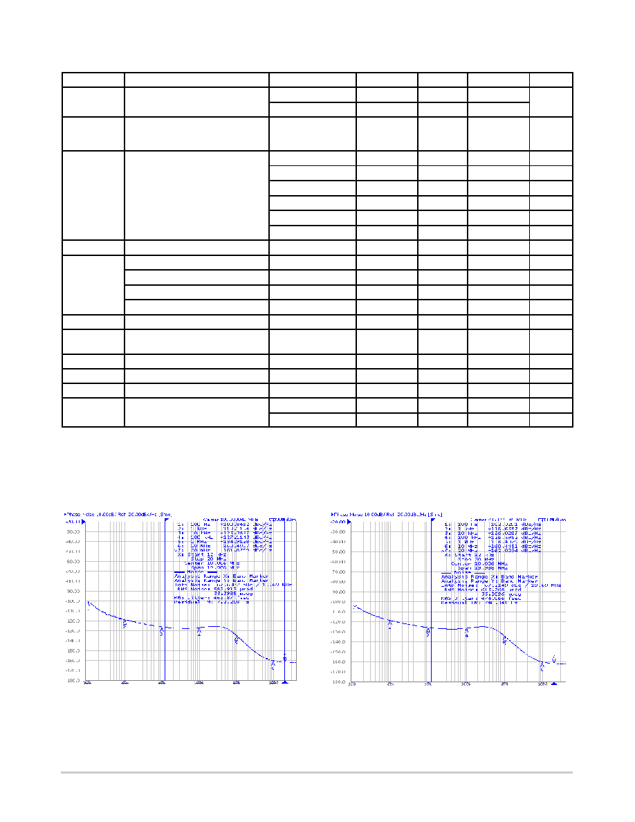
Figure 3. Typical Phase Noise Plot @ 200 MHz
Figure 4. Typical Phase Noise Plot @ 206.9 MHz
相关PDF资料 |
PDF描述 |
|---|---|
| VE-B4H-MY-S | CONVERTER MOD DC/DC 52V 50W |
| V300A3V3M200BL2 | CONVERTER MOD DC/DC 3.3V 200W |
| VE-B4F-MY-S | CONVERTER MOD DC/DC 72V 50W |
| VE-B4D-MY-S | CONVERTER MOD DC/DC 85V 50W |
| 74VHC139M | IC DECODER/DEMUX DL 2-4 16-SOIC |
相关代理商/技术参数 |
参数描述 |
|---|---|
| NBXDBA015LNHTAG | 功能描述:标准时钟振荡器 TRI FEQ LVPECL CLK OSC RoHS:否 制造商:AVX 产品:Standard Clock Oscillators 封装 / 箱体:7 mm x 5 mm 频率:75 MHz 频率稳定性:50 PPM 电源电压:2.5 V 负载电容: 端接类型:SMD/SMT 最小工作温度:0 C 最大工作温度:+ 70 C 输出格式:LVDS 尺寸: 封装:Reel 系列: |
| NBXDBA017 | 制造商:ONSEMI 制造商全称:ON Semiconductor 功能描述:Clock Oscillator |
| NBXDBA017LN1TAG | 功能描述:标准时钟振荡器 3.3V 156.25 312.5MHZ CLK RoHS:否 制造商:AVX 产品:Standard Clock Oscillators 封装 / 箱体:7 mm x 5 mm 频率:75 MHz 频率稳定性:50 PPM 电源电压:2.5 V 负载电容: 端接类型:SMD/SMT 最小工作温度:0 C 最大工作温度:+ 70 C 输出格式:LVDS 尺寸: 封装:Reel 系列: |
| NBXDBA017LNHTAG | 功能描述:标准时钟振荡器 156.25 312.5 MHZ 3.3V CLK RoHS:否 制造商:AVX 产品:Standard Clock Oscillators 封装 / 箱体:7 mm x 5 mm 频率:75 MHz 频率稳定性:50 PPM 电源电压:2.5 V 负载电容: 端接类型:SMD/SMT 最小工作温度:0 C 最大工作温度:+ 70 C 输出格式:LVDS 尺寸: 封装:Reel 系列: |
| NBXDBA018 | 制造商:ONSEMI 制造商全称:ON Semiconductor 功能描述:Clock Oscillator |
发布紧急采购,3分钟左右您将得到回复。