参数资料
| 型号: | NBXDPA019LNHTAG |
| 厂商: | ON Semiconductor |
| 文件页数: | 2/8页 |
| 文件大小: | 0K |
| 描述: | IC OSC XTAL 250MHZ 6-CLCC |
| 标准包装: | 1 |
| 系列: | PureEdge™ |
| 类型: | 振荡器 - 晶体 |
| 频率: | 125MHz,250MHz |
| 电源电压: | 2.375 V ~ 3.63 V |
| 电流 - 电源: | 78mA |
| 工作温度: | -40°C ~ 85°C |
| 封装/外壳: | 6-CLCC |
| 包装: | 标准包装 |
| 供应商设备封装: | 6-CLCC(7x5) |
| 安装类型: | 表面贴装 |
| 其它名称: | NBXDPA019LNHTAGOSDKR |
NBXDPA019
http://onsemi.com
2
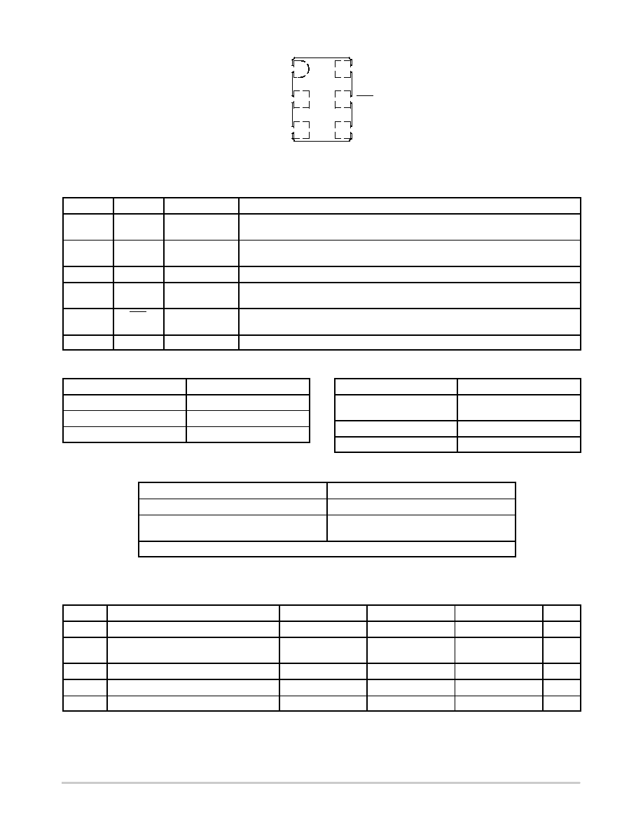
FSEL
OE
GND
CLK
VDD
CLK
1
2
3
6
5
4
Figure 2. Pin Connections (Top View)
Table 1. PIN DESCRIPTION
Pin No.
Symbol
I/O
Description
1
OE
LVTTL/LVCMOS
Control Input
Output Enable Pin. When left floating pin defaults to logic HIGH and output is active.
See OE pin description Table 2.
2
FSEL
LVTTL/LVCMOS
Control Input
Output Frequency Select Pin. Pin will default to logic HIGH when left open. See Output
Frequency Select pin description Table 3.
3
GND
Power Supply
Ground 0 V
4
CLK
LVDS Output
NonInverted Clock Output. Typically loaded with 100 W receiver termination resistor
across differential pair.
5
CLK
LVDS Output
Inverted Clock Output. Typically loaded with 100 W receiver termination resistor across
differential pair.
6
VDD
Power Supply
Positive power supply voltage. Voltage should not exceed 2.5 V ±5% or 3.3 V ±10%.
Table 2. OUTPUT ENABLE TRISTATE FUNCTION
OE Pin
Output Pins
Open
Active
HIGH Level
Active
LOW Level
High Z
Table 3. OUTPUT FREQUENCY SELECT
FSEL Pin
Output Frequency (MHz)
Open
(pin will float high)
125
HIGH Level
125
LOW Level
250
Table 4. ATTRIBUTES
Characteristic
Value
Input Default State Resistor
170 kW
ESD Protection
Human Body Model
Machine Model
2 kV
200 V
Meets or Exceeds JEDEC Standard EIA/JESD78 IC Latchup Test
1. For additional Moisture Sensitivity information, refer to Application Note AND8003/D.
Table 5. MAXIMUM RATINGS
Symbol
Parameter
Condition 1
Condition 2
Rating
Units
VDD
Positive Power Supply
GND = 0 V
4.6
V
Iout
LVDS Output Current
Continuous
Surge
25
50
mA
TA
Operating Temperature Range
40 to +85
°C
Tstg
Storage Temperature Range
55 to +120
°C
Tsol
Wave Solder
See Figure 6
260
°C
Stresses exceeding Maximum Ratings may damage the device. Maximum Ratings are stress ratings only. Functional operation above the
Recommended Operating Conditions is not implied. Extended exposure to stresses above the Recommended Operating Conditions may affect
device reliability.
相关PDF资料 |
PDF描述 |
|---|---|
| NBXHGA017LNHTAG | IC XO LVPECL 156.2500MHZ 6CLCC |
| NBXHGA019LNHTAG | IC XO LVPECL 125.0000MHZ 6CLCC |
| NBXHGA053LNHTAG | IC XO LVPECL 50.0000MHZ 6CLCC |
| NBXMBB024LNHTAG | IC XO LVPECL 622.08MHZ 6CLCC |
| NBXSBA007LNHTAG | IC OSC XTAL 240MHZ 6-CLCC |
相关代理商/技术参数 |
参数描述 |
|---|---|
| NBXDPA019LU1TAG | 功能描述:标准时钟振荡器 3.3V LVPECL PCIe, PCI Networking RoHS:否 制造商:AVX 产品:Standard Clock Oscillators 封装 / 箱体:7 mm x 5 mm 频率:75 MHz 频率稳定性:50 PPM 电源电压:2.5 V 负载电容: 端接类型:SMD/SMT 最小工作温度:0 C 最大工作温度:+ 70 C 输出格式:LVDS 尺寸: 封装:Reel 系列: |
| NBXHBA011LN1TAG | 功能描述:标准时钟振荡器 3.3V LVPECL Base station RoHS:否 制造商:AVX 产品:Standard Clock Oscillators 封装 / 箱体:7 mm x 5 mm 频率:75 MHz 频率稳定性:50 PPM 电源电压:2.5 V 负载电容: 端接类型:SMD/SMT 最小工作温度:0 C 最大工作温度:+ 70 C 输出格式:LVDS 尺寸: 封装:Reel 系列: |
| NBXHBA017 | 制造商:ONSEMI 制造商全称:ON Semiconductor 功能描述:Clock Oscillator |
| NBXHBA017LN1TAG | 功能描述:标准时钟振荡器 156.25MHZ LVPECL CLK 3.3V RoHS:否 制造商:AVX 产品:Standard Clock Oscillators 封装 / 箱体:7 mm x 5 mm 频率:75 MHz 频率稳定性:50 PPM 电源电压:2.5 V 负载电容: 端接类型:SMD/SMT 最小工作温度:0 C 最大工作温度:+ 70 C 输出格式:LVDS 尺寸: 封装:Reel 系列: |
| NBXHBA017LNHTAG | 功能描述:标准时钟振荡器 156.25MHZ 3.3V LVPECL CLK RoHS:否 制造商:AVX 产品:Standard Clock Oscillators 封装 / 箱体:7 mm x 5 mm 频率:75 MHz 频率稳定性:50 PPM 电源电压:2.5 V 负载电容: 端接类型:SMD/SMT 最小工作温度:0 C 最大工作温度:+ 70 C 输出格式:LVDS 尺寸: 封装:Reel 系列: |
发布紧急采购,3分钟左右您将得到回复。