- 您现在的位置:买卖IC网 > PDF目录9052 > NC7SZD384L6X (Fairchild Semiconductor)IC BUS SWITCH 1BIT LEVEL 6MCRPAK PDF资料下载
参数资料
| 型号: | NC7SZD384L6X |
| 厂商: | Fairchild Semiconductor |
| 文件页数: | 5/11页 |
| 文件大小: | 0K |
| 描述: | IC BUS SWITCH 1BIT LEVEL 6MCRPAK |
| 标准包装: | 5,000 |
| 系列: | 7SZ |
| 类型: | 总线开关 |
| 电路: | 1 x 1:1 |
| 独立电路: | 1 |
| 电压电源: | 单电源 |
| 电源电压: | 4.5 V ~ 5.5 V |
| 工作温度: | -40°C ~ 85°C |
| 安装类型: | 表面贴装 |
| 封装/外壳: | 6-UFDFN |
| 供应商设备封装: | Micro6?(TSOP-6) |
| 包装: | 带卷 (TR) |
3
www.fairchildsemi.com
NC7
SZ
D38
4
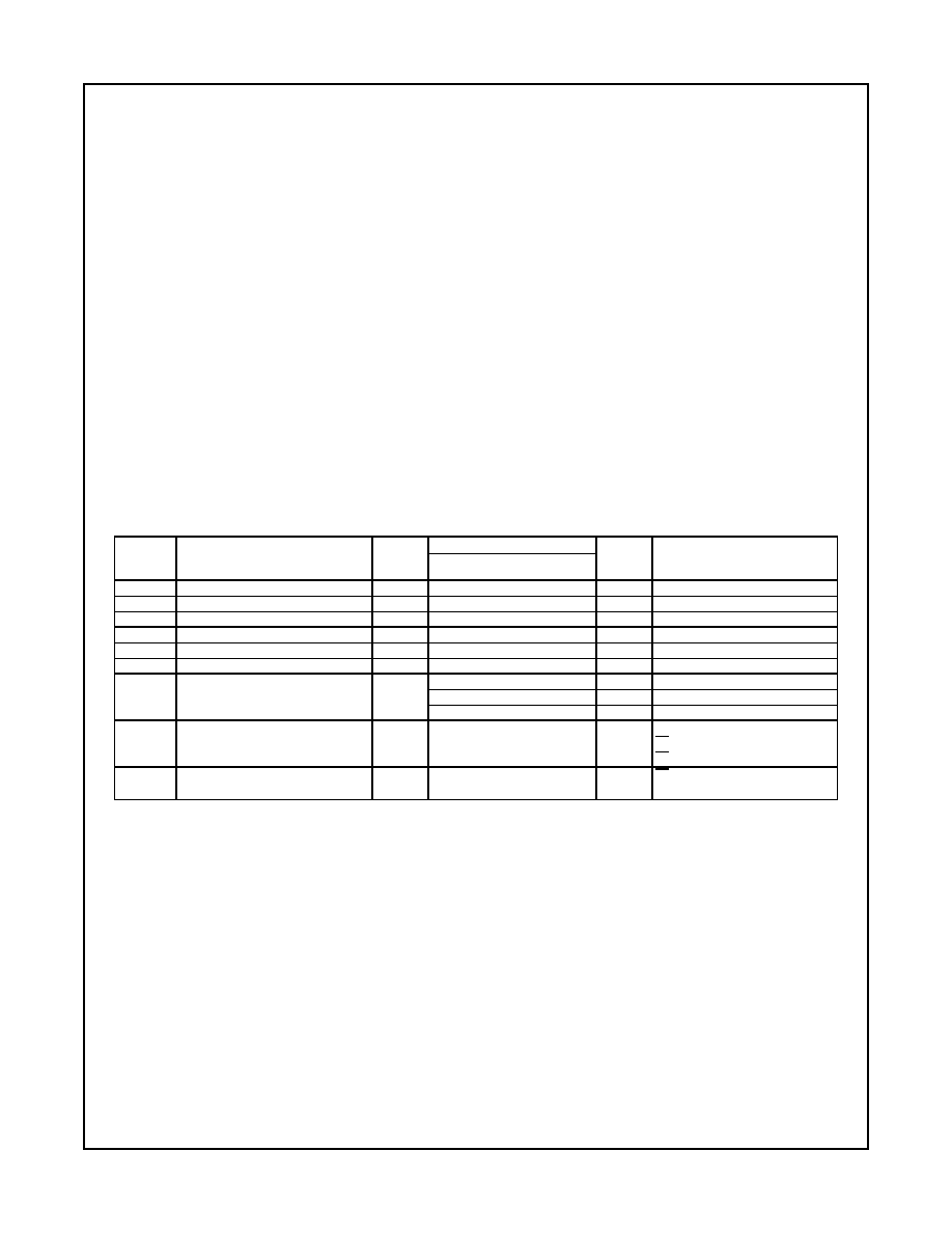
Absolute Maximum Ratings(Note 1)
Recommended Operating
Conditions (Note 3)
Note 1: The “Absolute Maximum Ratings” are those values beyond which the safety
of the device cannot be guaranteed. The device should not be operated at these lim-
its. The parametric values defined in the Electrical Characteristics tables are not
guaranteed at the absolute maximum ratings. The “Recommended Operating Condi-
tions” table will define the conditions for actual device operation.
Note 2: The input and output negative voltage ratings may be exceeded if the input
and output diode current ratings are observed.
Note 3: Unused inputs must be held HIGH or LOW. They may not float.
DC Electrical Characteristics
Note 4: All typical values are at VCC 5.0V, TA 25qC.
Note 5: Measured by the voltage drop between A and B pins at the indicated current through the switch. On Resistance is determined by the lower of the voltages on the two (A
or B) pins.
Note 6: Per TTL driven input (VIN 3.4V, control input only). A and B pins do not contribute to ICC.
Supply Voltage (VCC)
0.5V to 7.0V
DC Switch Voltage (VS)
0.5V to 7.0V
DC Input Voltage (VIN) (Note 2)
0.5V to 7.0V
DC Input Diode Current (IIK) VIN 0V
50 mA
DC Output (IOUT) Sink Current
128 mA
DC VCC/GND Current (ICC/GND)
r100 mA
Storage Temperature Range
(TSTG)
65qC to 150qC
Junction Temperature under bias (TJ)
150qC
Junction Lead Temperature (TL)
(Soldering, 10 seconds)
260qC
Power Dissipation (PD) @ 85qC
SOT23-5
200 mW
SC70-5
150 mW
Power Supply Operating (VCC)
4.5V to 5.5V
Input Voltage (VIN)
0V to 5.5V
Output Voltage (VOUT)
0V to 5.5V
Input Rise and Fall Time (tr, tf)
Switch Control Input
0 ns/V to 5 ns
Switch I/O
0 ns/V to DC
Operating Temperature (TA)
40qC to 85qC
Thermal Resistance (
TJA)
SOT23-5
300
qC/Watt
SC70-5
425
qC/Watt
Symbol
Parameter
VCC
TA 40qC to 85qC
Units
Conditions
(V)
Min
Typ
(Note 4)
Max
VIK
Maximum Clamp Diode Voltage
4.5
1.2
VIIN 18 mA
VIH
HIGH Level Input Voltage
4.5–5.5
2.0
V
VIL
LOW Level Input Voltage
4.5–5.5
0.8
V
VOH
HIGH Level Output Voltage
4.5–5.5
See Figure 3
V
VIN VCC
II
Input Leakage Current
0–5.5
r1.0
PA0 d VIN d 5.5V
IOFF
“OFF” Leakage Current
5.5
r10.0
PA0 d A, B, d VCC
RON
Switch On Resistance (Note 5)
4.5
5.0
7.0
:
VIN 0V, II 64 mA
5.0
7.0
:
VIN 0V, II 30 mA
35.0
50.0
:
VIN 2.4V, II 15 mA
ICC
Quiescent Supply Current
VIN VCC or GND, IO 0
Switch On
5.5
0.8
1.5
mA
OE
GND
Switch Off
5.5
10.0
PAOE VCC
'ICC
Increase in ICC per Input (Note 6)
5.5
0.8
2.5
mA
OE
3.4V, IO 0,
Control Input only.
相关PDF资料 |
PDF描述 |
|---|---|
| VE-JWY-MZ-F4 | CONVERTER MOD DC/DC 3.3V 16.5W |
| VI-2NL-MW-S | CONVERTER MOD DC/DC 28V 100W |
| VI-B5M-MY-F3 | CONVERTER MOD DC/DC 10V 50W |
| VI-26L-MW-S | CONVERTER MOD DC/DC 28V 100W |
| VI-B5M-MY-F1 | CONVERTER MOD DC/DC 10V 50W |
相关代理商/技术参数 |
参数描述 |
|---|---|
| NC7SZD384L6X_Q | 功能描述:数字总线开关 IC 1-Bit Bus Switch RoHS:否 制造商:Texas Instruments 开关数量:24 传播延迟时间:0.25 ns 最大工作温度:+ 85 C 最小工作温度:- 40 C 封装 / 箱体:TSSOP-56 封装:Reel |
| NC7SZD384M5 | 功能描述:数字总线开关 IC UHS 1-Bit Bus Switch RoHS:否 制造商:Texas Instruments 开关数量:24 传播延迟时间:0.25 ns 最大工作温度:+ 85 C 最小工作温度:- 40 C 封装 / 箱体:TSSOP-56 封装:Reel |
| NC7SZD384M5 | 制造商:Fairchild Semiconductor Corporation 功能描述:IC NC7SZ SMD 7SZD384 SOT-23-5 |
| NC7SZD384M57 | 制造商:Fairchild Semiconductor Corporation 功能描述: |
| NC7SZD384M5X | 功能描述:数字总线开关 IC UHS 1-Bit Bus Switch RoHS:否 制造商:Texas Instruments 开关数量:24 传播延迟时间:0.25 ns 最大工作温度:+ 85 C 最小工作温度:- 40 C 封装 / 箱体:TSSOP-56 封装:Reel |
发布紧急采购,3分钟左右您将得到回复。