参数资料
| 型号: | NCN2500MNR2 |
| 厂商: | ON Semiconductor |
| 文件页数: | 8/14页 |
| 文件大小: | 0K |
| 描述: | IC TXRX 1CHAN USB 16-QFN |
| 产品变化通告: | Discontinuation 30/Jun/2006 |
| 标准包装: | 3,000 |
| 类型: | 收发器 |
| 驱动器/接收器数: | 1/1 |
| 规程: | USB 2.0 |
| 电源电压: | 1.5 V ~ 3.6 V |
| 安装类型: | 表面贴装 |
| 封装/外壳: | 16-VFQFN 裸露焊盘 |
| 供应商设备封装: | 16-QFN(3x3) |
| 包装: | 带卷 (TR) |
NCN2500
http://onsemi.com
3
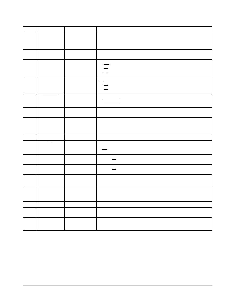
PIN FUNCTION DESCRIPTION
Pin
Symbol
Function
Description
1
DSPD
INPUT
The DSPD logic level (Data Speed) activates the Low or the High speed
operation on the USB port.
DSPD = Low
Low Speed, RPU1 and RPU2 connected to D
DSPD = High
Full Speed, RPU1 and RPU2 connected to D+
2
RCV
OUTPUT
This pin interfaces the USB signals with the microcontroller digital line. The data
present on the D+/D pins are translated onto this signal.
3
Vp
I/O
This pin, associated with Vm, is an I/O system interface signal depending upon
the OE logic state:
OE = Low
Vp is a Plus driver Input (from
mC to USB bus)
OE = High
Vp is a Plus receiver Output (from USB bus to
mC)
4
Vm
I/O
This pin, associated with Vp, is an I/O system interface signal depending upon the
OE logic state:
OE = Low
Vm is a Minus driver Input (from
mC to USB bus)
OE = High
Vm is a Minus receiver Output (from USB bus to
mC)
5
EN_VObus
INPUT
Digital input to control the VObus voltage.
EN_VObus = Low
VObus connected to Vreg
EN_VObus = High
VObus disconnected from Vreg (Hi Z)
6
GND
PWR
This pin carries the digital and USB ground level. High Quality PCB design shall
be observed to avoid uncontrolled voltage spikes.
7
SPND
INPUT
The SPND digital signal (SUSPEND) selects the operation mode to reduce the
power supply current.
SPND = Low
Normal operation
SPND = High
Suspend mode, no activity takes place
8
NC
No Connection, shall be neither grounded, nor connected to Vcc or Vbus.
9
OE
INPUT
This pin activates the operating mode of the D/D+ signals.
OE = Low logic level
Data are transmitted onto the USB bus
OE = High logic level
Data are received from the USB bus
10
D
I/O
This pin is connected to the USB Minus Data line I/O. The data direction depends
upon the OE logic state.
11
D+
I/O
This pin is connected to the USB Plus Data line I/O The data direction depends
upon the OE logic state.
12
Vreg
PWR
This pin provides a 3.3 V regulated voltage to supply the internal USB blocks and
the external termination bias resistor. An external circuit can be connected to this
LDO, assuming the current does not extend the maximum rating (50 mA).
13
VObus
OUTPUT, PWR
This pin connects the Vreg voltage to the 1.5 k external pullup resistor. The
VObus voltage is controlled by the logic states present Pin 5. The RDSon of the
internal PMOS device (reference S5 in the Block Diagram) is 10
W typical.
14
Vusb
PWR
This pin is connected to the USB port +Vcc supply voltage.
15
Vcc
PWR
This pin provides the interface power supply. The power source can be an
external supply or can be derived from the USB + Vusb voltage.
16
EN_RPU
INPUT
This pin activates or deactivate the internal RPU1 and RPU2 pullup resistors:
EN_RPU = H
RPU1 and RPU2 activated
EN_RPU = L
RPU1 and RPU2 deactivated
相关PDF资料 |
PDF描述 |
|---|---|
| MS27467T23A35PB | CONN PLUG 100POS STRAIGHT W/PINS |
| MC75174BPG | IC LINEDRVR QUAD EIA485 16-DIP |
| MC75174BDWG | IC LINEDRVR QUAD EIA485 20-SOICW |
| VI-B3B-MY-S | CONVERTER MOD DC/DC 95V 50W |
| MC75172BDWG | IC LINEDRIVER QUAD 3ST 20-SOICW |
相关代理商/技术参数 |
参数描述 |
|---|---|
| NCN2500MNR2G | 功能描述:总线收发器 USB Single Channel Transceiver RoHS:否 制造商:Fairchild Semiconductor 逻辑类型:CMOS 逻辑系列:74VCX 每芯片的通道数量:16 输入电平:CMOS 输出电平:CMOS 输出类型:3-State 高电平输出电流:- 24 mA 低电平输出电流:24 mA 传播延迟时间:6.2 ns 电源电压-最大:2.7 V, 3.6 V 电源电压-最小:1.65 V, 2.3 V 最大工作温度:+ 85 C 封装 / 箱体:TSSOP-48 封装:Reel |
| NCN25-F35-A2-250-15M-V1 | 制造商:PEPPERL+FUCHS 功能描述:Sensor, Proximity, M18, Inductive, 25mm Range, 10-30VDC, PNP, NO/NC, M12, 187480 制造商:PEPPERL+FUCHS 功能描述:Inductive DC |
| NCN25-F35-A2-250-V1 | 制造商:PEPPERL+FUCHS 功能描述:Sensor, Proximity, Inductive, DC 制造商:PEPPERL+FUCHS 功能描述:Inductive DC |
| NCN2612 | 制造商:ONSEMI 制造商全称:ON Semiconductor 功能描述:6-Differential Channel 1:2 Switch for PCIe 2.0 and Display Port 1.1 |
| NCN2612B | 制造商:ONSEMI 制造商全称:ON Semiconductor 功能描述:6-Channel Differential 1:2 Switch for PCIe 2.0 and Display Port 1.1 |
发布紧急采购,3分钟左右您将得到回复。