参数资料
| 型号: | NCN4557MTG |
| 厂商: | ON Semiconductor |
| 文件页数: | 2/12页 |
| 文件大小: | 0K |
| 描述: | IC SMART CARD/SIM DUAL 16-QFN |
| 产品变化通告: | Product Discontinuation 30/Sept/2011 |
| 标准包装: | 123 |
| 系列: | * |
| 应用: | * |
| 接口: | * |
| 电源电压: | * |
| 封装/外壳: | 16-WFQFN 裸露焊盘 |
| 供应商设备封装: | 16-QFN(3x3) |
| 包装: | 管件 |
| 安装类型: | 表面贴装 |
NCN4557
http://onsemi.com
10
18 k
CRD_I/O
14 k
I/O
VDD
LOGIC
IO/CONTROL
GND
200 ns
Q1
Q2
Q3
CRD_VCC
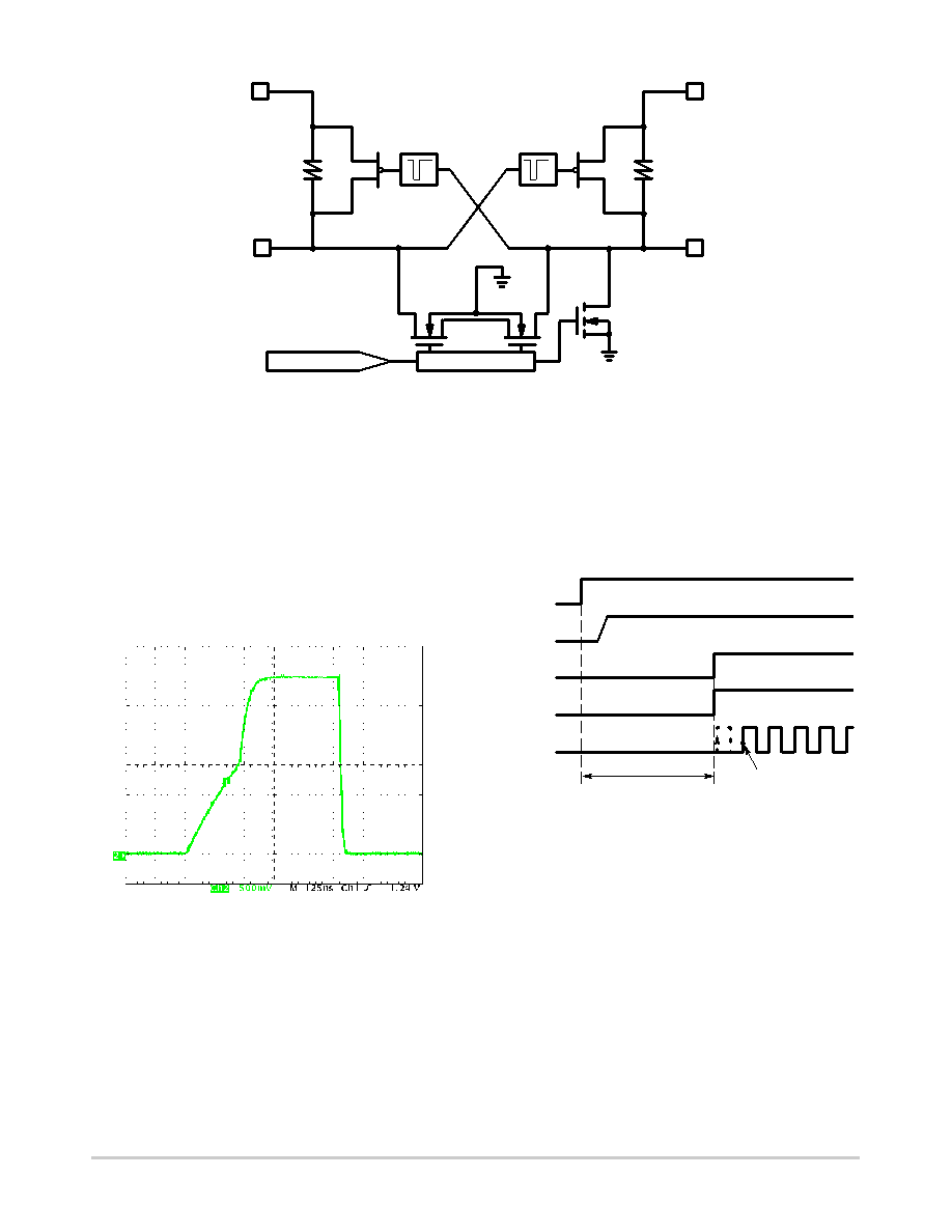
Figure 10. Basic I/O line Interface
The typical waveform provided in Figure 11 shows how
the accelerator operates. During the first 200 ns (typical),
the slope of the rise time is solely a function of the pullup
resistor associated with the stray capacitance. During this
period, the PMOS devices are not activated since the input
voltage is below their Vgs threshold. When the input slope
crosses the Vgsth, the opposite one shot is activated,
providing a low impedance to charge the capacitance, thus
increasing the rise time as depicted in Figure 11. The same
mechanism applies for the opposite side of the line to make
sure the system is optimum.
Figure 11. CRD_IO Typical Rise and Fall Times
with Stray Capacitance > 30 pF
(33 pF capacitor connected on the board)
Powerup Sequence
The powerup sequence makes sure all the cardrelated
signals are LOW during the CRD_VCC positive going
slope. The Powerup sequence is activated by setting the
ENABLE Boolean signal HIGH. CRD_RST, CRD_CLK
and CRD_I/O are maintained LOW during the activation
stage until CRD_VCC reaches its nominal value (1.8 V or
3.0 V). Figure 7 shows the typical NCN4557 activation
sequence.
About 800
ms after CRD_VCC has reached its nominal
voltage value, CRD_IO and CRD_RST are released.
CRD_CLK is enabled during the rising slope of the
second clock cycle after CRD_IO and CRD_RST are
enabled.
Figure 12. NCN4557 PowerUp
CRD_RSTA/B
CRD_IOA/B
CRD_CLKA/B
CRD_VCCA/B
ENABLE
TON ~ 0.9 ms
2nd Rise Edge After
CRD_IOA/B Rising
In all cases the application software is responsible for the
smart card signal sequence (contact activation sequence,
cold reset and warm reset sequences).
Powerdown Sequence
The NCN4557 provides a powerdown sequence which is
activated by setting the ENABLE Boolean signal LOW.
The communication I/O session is terminated immediately
according to the ISO7816 and EMV specifications as
ISO7816 Sequence:
CRD_RST is forced to LOW
CRD_CLK is forced to LOW 2 clock cycles after
ENABLE is set LOW unless CRD_CLK is already in
相关PDF资料 |
PDF描述 |
|---|---|
| NCN6000DTBR2G | IC INTERFACE SMART CARD 20TSSOP |
| NCN6001DTBR2 | IC INTERFACE SMART CARD 20TSSOP |
| NCN6004AFTBR2G | IC INTERFACE SAM/SIM DUAL 48TQFP |
| NCN6804MNR2G | IC SMART CARD DUAL W/SPI 32-QFN |
| NCN7200MTTWG | IC MUX/DEMUX OCTAL 1X2 42WQFN |
相关代理商/技术参数 |
参数描述 |
|---|---|
| NCN4557MTR2G | 功能描述:转换 - 电压电平 ANA DUAL SMART CARD INT RoHS:否 制造商:Micrel 类型:CML/LVDS/LVPECL to LVCMOS/LVTTL 传播延迟时间:1.9 ns 电源电流:14 mA 电源电压-最大:3.6 V 电源电压-最小:3 V 最大工作温度:+ 85 C 安装风格:SMD/SMT 封装 / 箱体:MLF-8 |
| NCN-4-8-2 | 制造商:z*INACTIVE* NATIONAL 功能描述: |
| NCN49597 | 制造商:ONSEMI 制造商全称:ON Semiconductor 功能描述:Power Line Carrier Modem |
| NCN49597ID11EVB | 制造商:ON Semiconductor 功能描述:EVAL BOARD - Bulk |
| NCN49597MNG | 功能描述:通信集成电路 - 若干 9.6 KBDS FLEX PLC MODEM RoHS:否 制造商:Maxim Integrated 类型:Transport Devices 封装 / 箱体:TECSBGA-256 数据速率:100 Mbps 电源电压-最大:1.89 V, 3.465 V 电源电压-最小:1.71 V, 3.135 V 电源电流:50 mA, 225 mA 最大工作温度:+ 85 C 最小工作温度:- 40 C 封装:Tube |
发布紧急采购,3分钟左右您将得到回复。