- 您现在的位置:买卖IC网 > PDF目录20446 > NCP1012GEVB (ON Semiconductor)EVAL BOARD FOR NCP1012G PDF资料下载
参数资料
| 型号: | NCP1012GEVB |
| 厂商: | ON Semiconductor |
| 文件页数: | 10/24页 |
| 文件大小: | 0K |
| 描述: | EVAL BOARD FOR NCP1012G |
| 设计资源: | NCP1012 Eval Brd BOM NCP1012GEVB Gerber Files NCP1012 Eval Brd Schematic |
| 标准包装: | 1 |
| 主要目的: | AC/DC,主面 |
| 输出及类型: | 1,隔离 |
| 输出电压: | 12V |
| 输入电压: | 230VAC |
| 稳压器拓扑结构: | 回扫 |
| 频率 - 开关: | 100kHz |
| 板类型: | 完全填充 |
| 已供物品: | 板 |
| 已用 IC / 零件: | NCP1012 |
| 其它名称: | NCP1012GEVBOS |
�� �
�
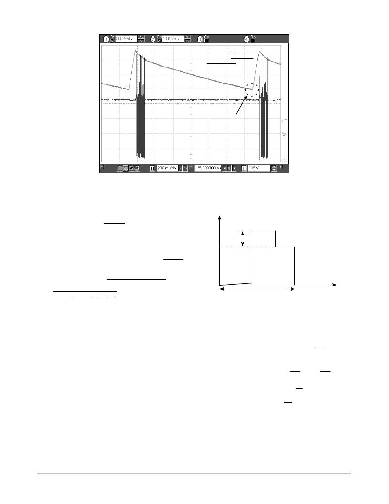
�NCP1010,� NCP1011,� NCP1012,� NCP1013,� NCP1014�
�Tsw�
�1� V� Ripple�
�Tstart�
�TLatch�
�Latch--off�
�Level�
�Figure� 16.� NCP101X� Facing� a� Fault� Condition� (Vin� =� 150� Vdc)�
�The� rising� slope� from� the� latch--off� level� up� to� 8.5� V�
�Vds(t)�
�is� expressed� by:� Tstart� =�
�.� The� time� during� which�
�.�
�the� IC� actually� pulses� is� given� by� tsw� =�
�Finally,� the� latch--off� time� can� be� derived�
�Δ� V1 · C�
�IC1�
�Δ� V2 · C�
�ICC1�
�Vin�
�Vr�
�toff�
�dt�
�.�
�using� the� same� formula� topology:� TLatch� =�
�Δ� V3 · C�
�ICC2�
�From� these� three� definitions,� the� burst� duty--cycle�
�(eq.� 2)� .�
�can� be� computed:� dc� =�
�(eq.� 3)� .�
�Feeding�
�the�
�dc� =�
�ICC1� ·� ?� ICC1� +� Δ� IC1� +� ICC2� ?�
�Tsw�
�Tstart� +� Tsw� +� TLatch�
�Δ� V2�
�Δ� V2� V1� Δ� V3�
�equation� with� values� extracted� from� the� parameter� section�
�gives� a� typical� duty--cycle� of� 13%,� precluding� any� lethal�
�ton�
�Tsw�
�Figure� 17.� A� typical� drain--ground� waveshape�
�where� leakage� effects� are� not� accounted� for.�
�t�
�<� Vds(t)� >=� Vin� ·� (1� ?� d)� +� Vr� ·� toff� (eq.� 5)�
�<� Vds(t)� >=� Vin� ?� Vin� ·� ton� +� Vr� ·� toff� (eq.� 6)�
�toff� can� be� expressed� by:� toff� =� Ip� ·�
�(eq.� 7)� where� ton�
�(eq.� 8)� .�
�can� be� evaluated� by:� ton� =� Ip� ·�
�thermal� runaway� while� in� a� fault� condition.�
�DSS� Internal� Dissipation�
�The� Dynamic� Self--Supplied� pulls� energy� out� from� the�
�drain� pin.� In� Flyback--based� converters,� this� drain� level� can�
�easily� go� above� 600� V� peak� and� thus� increase� the� stress� on� the�
�DSS� startup� source.� However,� the� drain� voltage� evolves� with�
�time� and� its� period� is� small� compared� to� that� of� the� DSS.� As�
�a� result,� the� averaged� dissipation,� excluding� capacitive� losses,�
�can� be� derived� by:� PDSS� =� ICC1� ·� <� Vds(t)� >� .� (eq.� 4)� .�
�Figure� 17� portrays� a� typical� drain--ground� waveshape� where�
�leakage� effects� have� been� removed.�
�By� looking� at� Figure� 17,� the� average� result� can� easily� be�
�derived� by� additive� square� area� calculation:�
�Tsw�
�By� developing� Equation� 5,� we� obtain:�
�Tsw� Tsw�
�Lp�
�Vr�
�Lp�
�Vin�
�http://onsemi.com�
�10�
�相关PDF资料 |
PDF描述 |
|---|---|
| R1S12-0505/HP | CONV DC/DC 1W 05VIN 05VOUT |
| 346-070-541-202 | CARDEDGE 70POS DUAL .125 GREEN |
| 1485E6 | WIREWAY 6" STEEL 8X8" GREY |
| R1S12-123.3/HP | CONV DC/DC 1W 12VIN 3.3VOUT |
| IPR-NIOS | IP NIOS II MEGACORE RENEW |
相关代理商/技术参数 |
参数描述 |
|---|---|
| NCP1012ST100T3 | 功能描述:电流型 PWM 控制器 Low Standby Power RoHS:否 制造商:Texas Instruments 开关频率:27 KHz 上升时间: 下降时间: 工作电源电压:6 V to 15 V 工作电源电流:1.5 mA 输出端数量:1 最大工作温度:+ 105 C 安装风格:SMD/SMT 封装 / 箱体:TSSOP-14 |
| NCP1012ST100T3G | 功能描述:电流型 PWM 控制器 Low Standby Power Monolithic Switcher RoHS:否 制造商:Texas Instruments 开关频率:27 KHz 上升时间: 下降时间: 工作电源电压:6 V to 15 V 工作电源电流:1.5 mA 输出端数量:1 最大工作温度:+ 105 C 安装风格:SMD/SMT 封装 / 箱体:TSSOP-14 |
| NCP1012ST130T3 | 功能描述:电流型 PWM 控制器 Low Standby Power RoHS:否 制造商:Texas Instruments 开关频率:27 KHz 上升时间: 下降时间: 工作电源电压:6 V to 15 V 工作电源电流:1.5 mA 输出端数量:1 最大工作温度:+ 105 C 安装风格:SMD/SMT 封装 / 箱体:TSSOP-14 |
| NCP1012ST130T3G | 功能描述:电流型 PWM 控制器 Low Standby Power Monolithic Switcher RoHS:否 制造商:Texas Instruments 开关频率:27 KHz 上升时间: 下降时间: 工作电源电压:6 V to 15 V 工作电源电流:1.5 mA 输出端数量:1 最大工作温度:+ 105 C 安装风格:SMD/SMT 封装 / 箱体:TSSOP-14 |
| NCP1012ST65T3 | 功能描述:电流型 PWM 控制器 Low Standby Power RoHS:否 制造商:Texas Instruments 开关频率:27 KHz 上升时间: 下降时间: 工作电源电压:6 V to 15 V 工作电源电流:1.5 mA 输出端数量:1 最大工作温度:+ 105 C 安装风格:SMD/SMT 封装 / 箱体:TSSOP-14 |
发布紧急采购,3分钟左右您将得到回复。