- 您现在的位置:买卖IC网 > PDF目录19694 > NCP1013ST65T3G (ON Semiconductor)IC OFFLINE SWIT SMPS CM SOT223 PDF资料下载
参数资料
| 型号: | NCP1013ST65T3G |
| 厂商: | ON Semiconductor |
| 文件页数: | 18/24页 |
| 文件大小: | 0K |
| 描述: | IC OFFLINE SWIT SMPS CM SOT223 |
| 标准包装: | 1 |
| 输出隔离: | 隔离 |
| 频率范围: | 59kHz ~ 71kHz |
| 输入电压: | 8.1 V ~ 10 V |
| 输出电压: | 700V |
| 功率(瓦特): | 19W |
| 工作温度: | -40°C ~ 125°C |
| 封装/外壳: | TO-261-4,TO-261AA |
| 供应商设备封装: | SOT-223 |
| 包装: | 剪切带 (CT) |
| 其它名称: | NCP1013ST65T3GOSCT |
�� �
�
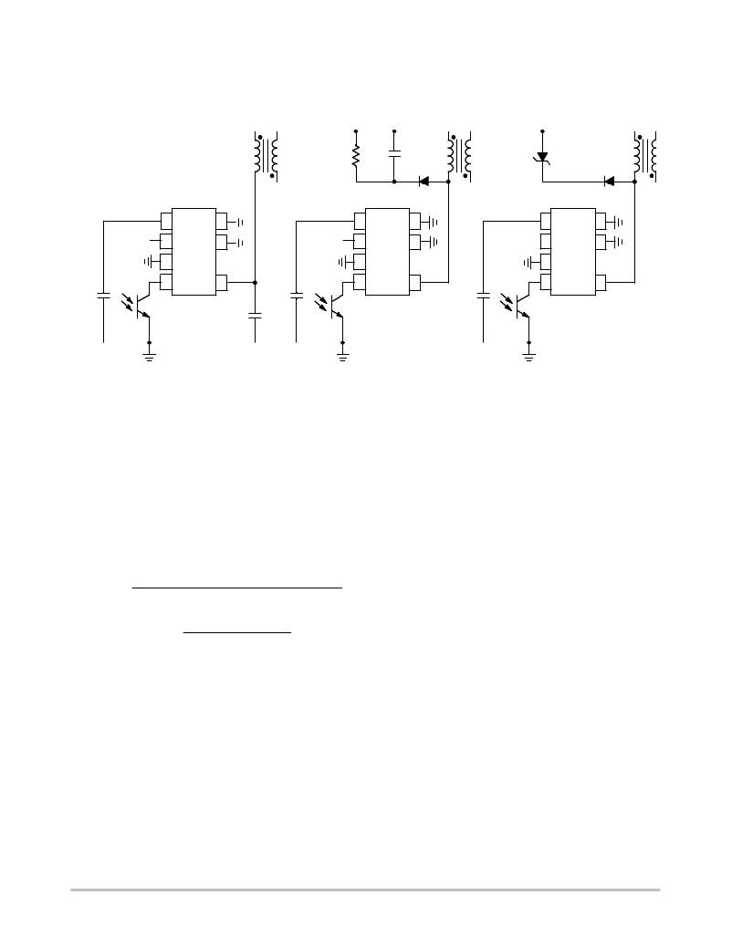
�NCP1010,� NCP1011,� NCP1012,� NCP1013,� NCP1014�
�MOSFET� Protection�
�As� in� any� Flyback� design,� it� is� important� to� limit� the�
�drain� excursion� to� a� safe� value,� e.g.� below� the� MOSFET�
�BV� DSS� which� is� 700� V.� Figure� 27� presents� possible�
�implementations:�
�HV�
�HV�
�HV�
�Rclamp�
�Cclamp�
�D�
�Dz�
�D�
�1�
�2�
�8�
�7�
�1�
�2�
�8�
�7�
�1�
�2�
�8�
�7�
�3�
�3�
�3�
�CVcc�
�+�
�4�
�NCP101X�
�5�
�CVcc�
�C�
�+�
�4�
�NCP101X�
�5�
�CVcc�
�+�
�4�
�NCP101X�
�5�
�A�
�B�
�Figure� 27.� Different� Options� to� Clamp� the� Leakage� Spike�
�C�
�Rclamp� =�
�Lleak� ·� Ip2� ·� Fsw�
�Vclamp�
�Cclamp� =�
�Figure� 27A� :� The� simple� capacitor� limits� the� voltage�
�according� to� Equation� 15.� This� option� is� only� valid� for� low�
�power� applications,� e.g.� below� 5.0� W,� otherwise� chances�
�exist� to� destroy� the� MOSFET.� After� evaluating� the� leakage�
�inductance,� you� can� compute� C� with� Equation� 15.� Typical�
�values� are� between� 100� pF� and� up� to� 470� pF.� Large�
�capacitors� increase� capacitive� losses.�
�Figure� 27B� :� This� diagram� illustrates� the� most� standard�
�circuitry� called� the� RCD� network.� Rclamp� and� Cclamp� are�
�calculated� using� the� following� formulas:�
�2 · Vclamp · (Vclamp� ?� (Vout� +� Vf sec) · N)�
�(eq.� 27)�
�(eq.� 28)�
�Vripple� ·� Fsw� ·� Rclamp�
�Vclamp� is� usually� selected� 50--80� V� above� the� reflected�
�Figure� 27C� :� This� option� is� probably� the� most� expensive� of�
�all� three� but� it� offers� the� best� protection� degree.� If� you� need�
�a� very� precise� clamping� level,� you� must� implement� a� Zener�
�diode� or� a� TVS.� There� are� little� technology� differences�
�behind� a� standard� Zener� diode� and� a� TVS.� However,� the� die�
�area� is� far� bigger� for� a� transient� suppressor� than� that� of� Zener.�
�A� 5.0� W� Zener� diode� like� the� 1N5388B� will� accept� 180� W�
�peak� power� if� it� lasts� less� than� 8.3� ms.� If� the� peak� current� in�
�the� worse� case� (e.g.� when� the� PWM� circuit� maximum�
�current� limit� works)� multiplied� by� the� nominal� Zener�
�voltage� exceeds� these� 180� W,� then� the� diode� will� be�
�destroyed� when� the� supply� experiences� overloads.� A�
�transient� suppressor� like� the� P6KE200� still� dissipates� 5.0� W�
�of� continuous� power� but� is� able� to� accept� surges� up� to� 600� W�
�@� 1.0� ms.� Select� the� Zener� or� TVS� clamping� level� between�
�40� to� 80� V� above� the� reflected� output� voltage� when� the�
�supply� is� heavily� loaded.�
�value� N� x� (Vout� +� Vf).� The� diode� needs� to� be� a� fast� one� and�
�a� MUR160� represents� a� good� choice.� One� major� drawback�
�of� the� RCD� network� lies� in� its� dependency� upon� the� peak�
�current.� Worse� case� occurs� when� Ip� and� Vin� are� maximum�
�and� Vout� is� close� to� reach� the� steady--state� value.�
�http://onsemi.com�
�18�
�相关PDF资料 |
PDF描述 |
|---|---|
| VI-B4P-CY-F1 | CONVERTER MOD DC/DC 13.8V 50W |
| ACM30DRMI | CONN EDGECARD 60POS .156 SQ WW |
| TAP335K035CRW | CAP TANT 3.3UF 35V 10% RADIAL |
| VI-B4N-CY-F4 | CONVERTER MOD DC/DC 18.5V 50W |
| MIC5203-2.8BM4 TR | IC REG LDO 2.8V 80MA SOT-143 |
相关代理商/技术参数 |
参数描述 |
|---|---|
| NCP1014 | 制造商:ONSEMI 制造商全称:ON Semiconductor 功能描述:Self-Supplied Monolithic Switcher for Low Standby- Power Offline SMPS |
| NCP1014/D | 制造商:未知厂家 制造商全称:未知厂家 功能描述:Self-Supplied Monolithic Switcher for Low Standby-Power Offline SMPS |
| NCP1014AP065 | 功能描述:电流型 PWM 控制器 Low Standby Power RoHS:否 制造商:Texas Instruments 开关频率:27 KHz 上升时间: 下降时间: 工作电源电压:6 V to 15 V 工作电源电流:1.5 mA 输出端数量:1 最大工作温度:+ 105 C 安装风格:SMD/SMT 封装 / 箱体:TSSOP-14 |
| NCP1014AP065G | 功能描述:电流型 PWM 控制器 Low Standby Power Monolithic Switcher RoHS:否 制造商:Texas Instruments 开关频率:27 KHz 上升时间: 下降时间: 工作电源电压:6 V to 15 V 工作电源电流:1.5 mA 输出端数量:1 最大工作温度:+ 105 C 安装风格:SMD/SMT 封装 / 箱体:TSSOP-14 |
| NCP1014AP10 | 制造商:ONSEMI 制造商全称:ON Semiconductor 功能描述:Self-Supplied Monolithic Switcher for Low Standby- Power Offline SMPS |
发布紧急采购,3分钟左右您将得到回复。