- 您现在的位置:买卖IC网 > PDF目录22030 > NCP1086T-ADJ (ON Semiconductor)IC REG LDO ADJ 1.5A TO220AB PDF资料下载
参数资料
| 型号: | NCP1086T-ADJ |
| 厂商: | ON Semiconductor |
| 文件页数: | 7/13页 |
| 文件大小: | 0K |
| 描述: | IC REG LDO ADJ 1.5A TO220AB |
| 产品变化通告: | Product Discontinuation 27/Jun/2007 |
| 标准包装: | 50 |
| 稳压器拓扑结构: | 正,可调式 |
| 输出电压: | 1.25 V ~ 5.5 V |
| 输入电压: | 最高 7V |
| 电压 - 压降(标准): | 1.05V @ 1.5A |
| 稳压器数量: | 1 |
| 电流 - 输出: | 1.5A |
| 电流 - 限制(最小): | 1.6A |
| 工作温度: | 0°C ~ 70°C |
| 安装类型: | 通孔 |
| 封装/外壳: | TO-220-3 |
| 供应商设备封装: | TO-220AB |
| 包装: | 管件 |
| 其它名称: | NCP1086T-ADJOS |
�� �
�
�NCP1086�
�Protection� Diodes�
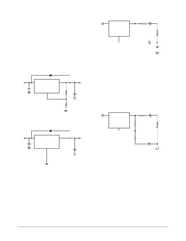
�When� large� external� capacitors� are� used� with� a� linear�
�regulator� it� is� sometimes� necessary� to� add� protection� diodes.�
�V� IN�
�V� IN�
�V� OUT�
�R� C�
�Conductor� Parasitic�
�Resistance�
�If� the� input� voltage� of� the� regulator� gets� shorted,� the� output�
�capacitor� will� discharge� into� the� output� of� the� regulator.� The�
�discharge� current� depends� on� the� value� of� the� capacitor,� the�
�output� voltage� and� the� rate� at� which� V� IN� drops.� In� the�
�NCP1086� series� linear� regulator,� the� discharge� path� is�
�through� a� large� junction� and� protection� diodes� are� not�
�usually� needed.� If� the� regulator� is� used� with� large� values� of�
�output� capacitance� and� the� input� voltage� is� instantaneously�
�shorted� to� ground,� damage� can� occur.� In� this� case,� a� diode�
�connected� as� shown� in� Figure� 17� or� Figure� 18� is�
�recommended.�
�NCP1086�
�R� LOAD�
�Figure� 19.� Conductor� Parasitic� Resistance� Effects�
�Can� Be� Minimized� with� the� Above� Grounding�
�Scheme� for� Fixed� Output� Regulators�
�For� the� adjustable� regulator,� the� best� load� regulation�
�RC�
�V� IN�
�C� 1�
�V� IN�
�IN4002� (optional)�
�V� OUT�
�NCP1086�
�Adj�
�R� 1�
�C� 2�
�V� OUT�
�occurs� when� R1� is� connected� directly� to� the� output� pin� of� the�
�regulator� as� shown� in� Figure� 20.� If� R1� is� connected� to� the�
�load,� R� C� is� multiplied� by� the� divider� ratio� and� the� effective�
�resistance� between� the� regulator� and� the� load� becomes�
�R1� )� R2�
�R1�
�R� 2�
�where� R� C� =� conductor� parasitic� resistance.�
�Conductor� Parasitic�
�Figure� 17.� Protection� Diode� Scheme� for� Large� Output�
�Capacitors� (Adjustable� Output)�
�V� IN�
�V� IN�
�V� OUT�
�NCP1086�
�Adj�
�R� 1�
�R� C�
�Resistance�
�R� LOAD�
�IN4002� (optional)�
�V� IN�
�C� 1�
�V� IN�
�NCP1086�
�GND�
�V� OUT�
�C� 2�
�V� OUT�
�R� 2�
�Figure� 20.� Grounding� Scheme� for� the�
�Adjustable� Output� Regulator� to� Minimize�
�Parasitic� Resistance� Effects�
�Figure� 18.� Protection� Diode� Scheme� for� Large� Output�
�Capacitors� (3.3� V� Fixed� Output)�
�Calculating� Power� Dissipation� and�
�Output� Voltage� Sensing�
�Since� the� NCP1086� is� a� three� terminal� regulator,� it� is� not�
�possible� to� provide� true� remote� load� sensing.� Load�
�regulation� is� limited� by� the� resistance� of� the� conductors�
�connecting� the� regulator� to� the� load.�
�For� best� results� the� fixed� output� regulator� should� be�
�connected� as� shown� in� Figure� 19.�
�Heatsink� Requirements�
�The� NCP1086� linear� regulator� includes� thermal� shutdown�
�and� current� limit� circuitry� to� protect� the� device.� High� power�
�regulators� such� as� these� usually� operate� at� high� junction�
�temperatures� so� it� is� important� to� calculate� the� power�
�dissipation� and� junction� temperatures� accurately� to� ensure�
�that� an� adequate� heatsink� is� used.�
�http://onsemi.com�
�7�
�相关PDF资料 |
PDF描述 |
|---|---|
| ADT7467ARQZ | IC PWM FAN CTRLR W/MONITR 16QSOP |
| D09P13A4PL00LF | CONN DSUB PLUG 9 POS R/A GOLD |
| VE-BWD-CV-F3 | CONVERTER MOD DC/DC 85V 150W |
| ADT7461ARZ | IC TEMP MONITOR +/-1C DUAL 8SOIC |
| VE-BWD-CV-F2 | CONVERTER MOD DC/DC 85V 150W |
相关代理商/技术参数 |
参数描述 |
|---|---|
| NCP1086T-ADJG | 功能描述:低压差稳压器 - LDO 1.25-5.5V ADJ 1.5A Commercial Temp RoHS:否 制造商:Texas Instruments 最大输入电压:36 V 输出电压:1.4 V to 20.5 V 回动电压(最大值):307 mV 输出电流:1 A 负载调节:0.3 % 输出端数量: 输出类型:Fixed 最大工作温度:+ 125 C 安装风格:SMD/SMT 封装 / 箱体:VQFN-20 |
| NCP1090 | 制造商:ONSEMI 制造商全称:ON Semiconductor 功能描述:Integrated IEEE 802.3af PoE-PD Interface Controller |
| NCP1090DBG | 功能描述:开关变换器、稳压器与控制器 HINT OAA TSSOP8 NCP1090DB RoHS:否 制造商:Texas Instruments 输出电压:1.2 V to 10 V 输出电流:300 mA 输出功率: 输入电压:3 V to 17 V 开关频率:1 MHz 工作温度范围: 安装风格:SMD/SMT 封装 / 箱体:WSON-8 封装:Reel |
| NCP1090DBRG | 功能描述:开关变换器、稳压器与控制器 HINT OAA TSSOP8 NCP1090DB RoHS:否 制造商:Texas Instruments 输出电压:1.2 V to 10 V 输出电流:300 mA 输出功率: 输入电压:3 V to 17 V 开关频率:1 MHz 工作温度范围: 安装风格:SMD/SMT 封装 / 箱体:WSON-8 封装:Reel |
| NCP1090DG | 功能描述:开关变换器、稳压器与控制器 HINT OAA SOIC8 RoHS:否 制造商:Texas Instruments 输出电压:1.2 V to 10 V 输出电流:300 mA 输出功率: 输入电压:3 V to 17 V 开关频率:1 MHz 工作温度范围: 安装风格:SMD/SMT 封装 / 箱体:WSON-8 封装:Reel |
发布紧急采购,3分钟左右您将得到回复。