- 您现在的位置:买卖IC网 > PDF目录11583 > NCP1092DG (ON Semiconductor)IC INTERFACE CTLR POE-PD 8-SOIC PDF资料下载
参数资料
| 型号: | NCP1092DG |
| 厂商: | ON Semiconductor |
| 文件页数: | 11/12页 |
| 文件大小: | 0K |
| 描述: | IC INTERFACE CTLR POE-PD 8-SOIC |
| 标准包装: | 96 |
| 系列: | HIPO™ |
| 控制器类型: | PoE-PD 接口 |
| 接口: | IEEE 802.3af |
| 电流 - 电源: | 500mA |
| 工作温度: | -40°C ~ 85°C |
| 安装类型: | 表面贴装 |
| 封装/外壳: | 8-SOIC(0.154",3.90mm 宽) |
| 供应商设备封装: | 8-SOIC |
| 包装: | 散装 |
| 其它名称: | NCP1092DGOS |
NCP1090, NCP1091, NCP1092
http://onsemi.com
8
Example for a Targeted Uvlo_on of 35 V:
Let’s start with a Rdet of 30.1 k
Ω. This gives a Ruvlo of
144 k
Ω made with a Ruvlo2 of 4.99 kΩ and a Ruvlo1 of
140 k
Ω (closest values from E96 series). Note that there is
a pull down current of 2.5
mA typ on the UVLO. Assuming
the previous example, this pull down current will create a
(non critical) systematic offset of 350 mV on the Uvlon_on
level of 35 V.
The external UVLO hysteresis on the NCP1091 is about
15 percent typical.
Inrush and Operational Current Limitations
Both inrush and operational current limit are defined by
an external Rinrush resistor connected between INRUSH
and VPORTN. The low inrush current limit allows smooth
charge of large dcdc converter input capacitor by limiting
the power dissipation over the internal pass switch. In power
mode, the operational current limit protects the pass switch
and the PD application against excessive transient current
and failure on the dcdc converter output.
Once the input supply reached the Vulvo_on level, the
charge of Cpd capacitor starts with a current limitation set to
to the INRUSH level. When this capacitor is fully charged,
the current limit switches without any spikes from the inrush
current to the operational current level and the power good
indicator on PGOOD pin is turned on. The capacitor is
considered to be fully charged once the following conditions
are satisfied:
1. The drainsource voltage of the Pass Switch has
decreased below the Vds_pgood_on level (typical
1V)
2. The gatesource voltage of the Pass Switch is
sufficiently high (above 2 V typical) which means
the current in the pass switch has decreased below
the current limit.
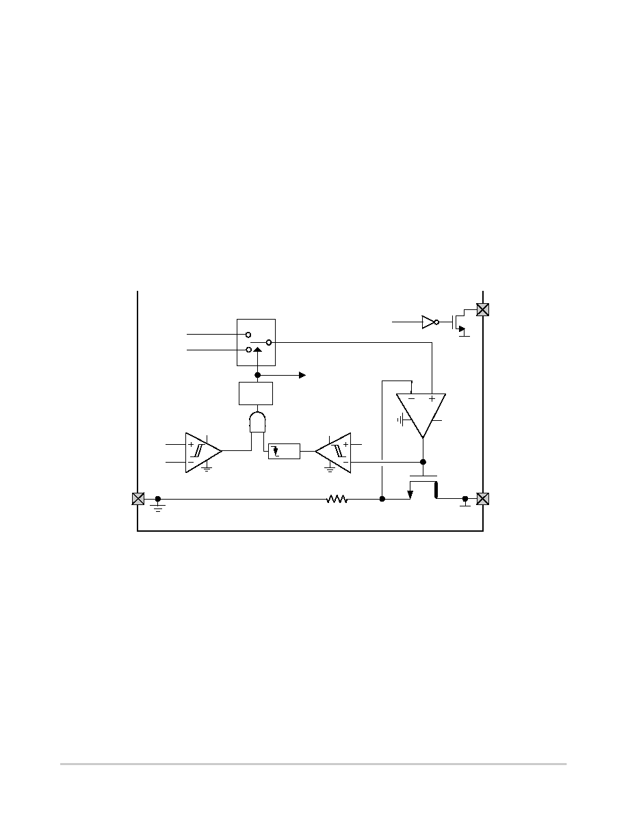
This mechanism is depicted in the following Figure 7.
Operational current limit
VPORTNx
Pass Switch
Inrush current limit
RTN
0
1
VDDA1
1 V / 10 V
2 V
Delay
&
detector
PGOOD
Pgood_on
VDDA1
RTN
Pgood_on
Sense Resistor
Vds_pgood comparator
Vgs_pgood comparator
Figure 7. Inrush and Operational Current Limitation Selection Mechanism
100 mS
The operational current limit and the power good
indicator stays active as long as RTN voltage stays below the
vds_pgood_off threshold (10 V typical) and the input supply
stay above the Vulvo_off level. Therefore, fast and large
voltage step lower than 10 V are tolerated on the input
without interruption of the converter controller. Higher
input transient will not affect the behavior if RTN does not
exceed 10 V for more than 100
mS. Such input voltage steps
may be introduced by a PSE which is switched to a higher
power supply. In case RTN is still above 10 V after this delay,
the power good is turned off and the pass switch current limit
falls back to the inrush level.
PGOOD Indicator
The NCP1090/91/92 integrate a Power Good indicator
circuitry indicating the end of the dcdc converter input
capacitor charge, and the enabling of the operational current
limit. This indicator is implemented on the PGOOD pin
which goes in open drain state when active and which is
pulled to ground during turn off.
A possible usage of this PGOOD pin is illustrated in
Figure 8. During the inrush phase, the converter controller
is forced in standby mode due to the PGOOD pin forcing low
the under voltage lock out pin of the controller. Once the Cpd
capacitor is fully charged, PGOOD goes in open drain state,
allowing the start up sequence of the converter controller.
相关PDF资料 |
PDF描述 |
|---|---|
| NCP1090DG | IC INTERFACE CTLR POE-PD 8-SOIC |
| V150A8C400BF | CONVERTER MOD DC/DC 8V 400W |
| V150A8C400BL3 | CONVERTER MOD DC/DC 8V 400W |
| V150A8C400BL2 | CONVERTER MOD DC/DC 8V 400W |
| V150A8C400B3 | CONVERTER MOD DC/DC 8V 400W |
相关代理商/技术参数 |
参数描述 |
|---|---|
| NCP1092DRG | 功能描述:开关变换器、稳压器与控制器 HINT O1A SOIC8 RoHS:否 制造商:Texas Instruments 输出电压:1.2 V to 10 V 输出电流:300 mA 输出功率: 输入电压:3 V to 17 V 开关频率:1 MHz 工作温度范围: 安装风格:SMD/SMT 封装 / 箱体:WSON-8 封装:Reel |
| NCP1093MNG | 功能描述:热插拔功率分布 RoHS:否 制造商:ON Semiconductor 产品: 电流限制: 电源电压-最大: 电源电压-最小: 工作温度范围: 功率耗散: 安装风格: 封装 / 箱体: 封装: |
| NCP1093MNRG | 功能描述:热插拔功率分布 HINT OAA DFN10 NCP1093MNG RoHS:否 制造商:Texas Instruments 产品:Controllers & Switches 电流限制: 电源电压-最大:7 V 电源电压-最小:- 0.3 V 工作温度范围: 功率耗散: 安装风格:SMD/SMT 封装 / 箱体:MSOP-8 封装:Tube |
| NCP1094GEVB | 制造商:ON Semiconductor 功能描述:AE- INDUSTRIAL PRODUCTS - Bulk |
| NCP1094MNG | 制造商:ON Semiconductor 功能描述:HINT OAC DFN10 NCP1094MNG - Bulk |
发布紧急采购,3分钟左右您将得到回复。