- 您现在的位置:买卖IC网 > PDF目录11568 > NCP1092DRG (ON Semiconductor)IC INTERFACE CTLR POE-PD 8-SOIC PDF资料下载
参数资料
| 型号: | NCP1092DRG |
| 厂商: | ON Semiconductor |
| 文件页数: | 7/12页 |
| 文件大小: | 0K |
| 描述: | IC INTERFACE CTLR POE-PD 8-SOIC |
| 标准包装: | 1 |
| 系列: | HIPO™ |
| 控制器类型: | PoE-PD 接口 |
| 接口: | IEEE 802.3af |
| 电流 - 电源: | 500mA |
| 工作温度: | -40°C ~ 85°C |
| 安装类型: | 表面贴装 |
| 封装/外壳: | 8-SOIC(0.154",3.90mm 宽) |
| 供应商设备封装: | 8-SOIC |
| 包装: | 标准包装 |
| 其它名称: | NCP1092DRGOSDKR |
NCP1090, NCP1091, NCP1092
http://onsemi.com
4
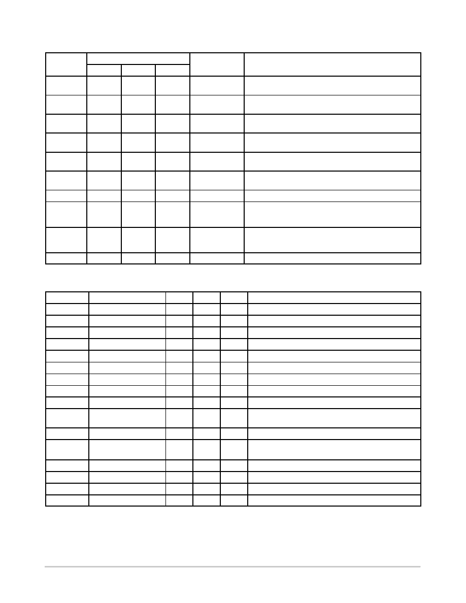
Table 1. PIN DESCRIPTION
Name
Pin No.
Type
Description
NCP1090
NCP1091
NCP1092
INRUSH
1
Output
Current limit programming pin. Connect a resistor between
INRUSH and VPORTN.
CLASS
2
Output
Classification current programming pin. Connect a resistor
between CLASS and VPORTN.
DET
3
Output,
Open Drain
Detection pin. Connect a 24.9 kW resistor between DET and
VPORTP for a valid PD detection signature.
VPORTN
4
Ground
Negative input power. Connected to the source of the internal
passswitch
RTN
5
Ground
DCDC controller power return. Connected to the drain of the
internal passswitch
PGOOD
6
Output,
Open Drain
Open Drain Power Good Indicator. Pin is in HZ mode when the
power good signal is active.
NC
7
No connection
UVLO
7
Input
Undervoltage lockout input. Voltage with respect to VPORTN.
Connect a resistordivider from VPORTP to UVLO to
VPORTNx to set an external UVLO threshold.
AUX
7
Input
Auxiliary Pin. When this pin is pulled up, the Pass Switch is
disabled and allows a supply transition from PSE to the rear
auxiliary supply connected between VPORTP and RTN.
VPORTP
8
Input
Positive input power. Voltage with respect to VPORTN.
Operating Conditions
Table 2. ABSOLUTE MAXIMUM RATINGS
Symbol
Parameter
Min
Max
Units
Conditions
VPORTP
Input power supply
0.3
72
V
Voltage with respect to VPORTN
RTN
Analog ground supply 2
0.3
72
V
Passswitch in offstate (voltage with respect to VPORTN)
CLASS
Analog output
0.3
72
V
Voltage with respect to VPORTN
INRUSH
Analog output
0.3
3.6
V
Voltage with respect to VPORTN
AUX
Analog input
0.3
72
V
Voltage with respect to VPORTN
UVLO
Analog input
0.3
3.6
V
Voltage with respect to VPORTN
PGOOD
Analog output
0.3
72
V
Voltage with respect to RTN
Ta
Ambient temperature
40
85
°C
Tj
Junction temperature
125
°C
TjTSD
Junction temperature
(Note 1)
175
°C
Thermal shutdown condition
Tstg
Storage Temperature
55
150
°C
TθJA
Thermal Resistance,
Junction to Air (Note 2)
150
160
240
260
°C/W
SOIC8
TSSOP8
ESDHBM
Human Body Model
2
kV
per EIAJESD22A114 standard
ESDCDM
Charged Device Model
500
V
per ESDSTM5.3.1 standard
ESDMM
Machine Model
200
V
per EIAJESD22A115A standard
LU
Latchup
±100
mA
per JEDEC Standard JESD78
Stresses exceeding Maximum Ratings may damage the device. Maximum Ratings are stress ratings only. Functional operation above the
Recommended Operating Conditions is not implied. Extended exposure to stresses above the Recommended Operating Conditions may affect
device reliability.
1. TjTSD allowed during error conditions only. It is assumed that this maximum temperature condition does not occur more than 1 hour
cumulative during the useful life for reliability reasons.
2. Low qJA is obtained with 2S2P test board (2 signal 2 plane). High qJA is obtained with double sideboard with minimum pad area and natural
convection. Refer to Jedec JESD51 for details.
相关PDF资料 |
PDF描述 |
|---|---|
| V375C3V3M50B | CONVERTER MOD DC/DC 3.3V 50W |
| V375A3V3C264BG3 | CONVERTER MOD DC/DC 3.3V 264W |
| V375A3V3C264BG2 | CONVERTER MOD DC/DC 3.3V 264W |
| V375A3V3C264BG | CONVERTER MOD DC/DC 3.3V 264W |
| NCP1091DRG | IC INTERFACE CTLR POE-PD 8-TSSOP |
相关代理商/技术参数 |
参数描述 |
|---|---|
| NCP1093MNG | 功能描述:热插拔功率分布 RoHS:否 制造商:ON Semiconductor 产品: 电流限制: 电源电压-最大: 电源电压-最小: 工作温度范围: 功率耗散: 安装风格: 封装 / 箱体: 封装: |
| NCP1093MNRG | 功能描述:热插拔功率分布 HINT OAA DFN10 NCP1093MNG RoHS:否 制造商:Texas Instruments 产品:Controllers & Switches 电流限制: 电源电压-最大:7 V 电源电压-最小:- 0.3 V 工作温度范围: 功率耗散: 安装风格:SMD/SMT 封装 / 箱体:MSOP-8 封装:Tube |
| NCP1094GEVB | 制造商:ON Semiconductor 功能描述:AE- INDUSTRIAL PRODUCTS - Bulk |
| NCP1094MNG | 制造商:ON Semiconductor 功能描述:HINT OAC DFN10 NCP1094MNG - Bulk |
| NCP1094MNRG | 功能描述:热插拔功率分布 HINT OAA DFN10 NCP1094MNG RoHS:否 制造商:Texas Instruments 产品:Controllers & Switches 电流限制: 电源电压-最大:7 V 电源电压-最小:- 0.3 V 工作温度范围: 功率耗散: 安装风格:SMD/SMT 封装 / 箱体:MSOP-8 封装:Tube |
发布紧急采购,3分钟左右您将得到回复。