- 您现在的位置:买卖IC网 > PDF目录19528 > NCP1201P100 (ON Semiconductor)IC CTRLR PWM CM OTP 8DIP PDF资料下载
参数资料
| 型号: | NCP1201P100 |
| 厂商: | ON Semiconductor |
| 文件页数: | 14/19页 |
| 文件大小: | 0K |
| 描述: | IC CTRLR PWM CM OTP 8DIP |
| 产品变化通告: | LTB Notification 03/Jan/2008 |
| 标准包装: | 1,000 |
| 输出隔离: | 隔离 |
| 频率范围: | 92kHz ~ 117kHz |
| 输入电压: | 12.5 V ~ 16 V |
| 输出电压: | 500V |
| 工作温度: | -40°C ~ 150°C |
| 封装/外壳: | 8-DIP(0.300",7.62mm) |
| 供应商设备封装: | 8-PDIP |
| 包装: | 管件 |
�� �
�
�NCP1201�
�APPLICATION� INFORMATION�
�=� 750� mW� (T� Jmax� =� 125� _� C),�
�P� max� =�
�� 1.6� mA� =� 356.5� mW� .�
�350� V� � 2�
�lower� the� dissipation� to�
�Power� Dissipation�
�The� NCP1201� can� be� directly� supplied� from� the� DC� rail�
�through� the� internal� DSS� circuitry.� The� average� current�
�flowing� through� the� DSS� is� therefore� the� direct� image� of� the�
�NCP1201� current� consumption.� The� total� power� dissipation�
�can� be� evaluated� using:� (VHVDC� ?� 11� V)� � ICC2� .� If� the�
�device� operates� on� a� 250� VAC� rail,� the� maximum� rectified�
�voltage� can� go� up� to� 350� VDC.� At� T� A� =� 25� ?� C,� I� CC2� =� 2.1� mA�
�for� the� 60� kHz� version� over� a� 1.0� nF� capacitive� load.� As� a�
�result,� the� NCP1201� will� dissipate� 350� V� x� 2.1� mA� =�
�735� mW� (T� A� =� 25� _� C).� The� SOIC--8� package� offers� a�
�junction--to--ambient� thermal� resistance� R� θ� J--A� of� 178� ?� C/W.�
�Adding� some� copper� area� around� the� device� pins� will� help�
�to� improve� this� number,� 12mm� x� 12mm� copper� can� drop�
�R� θ� J--A� down� to� 100� ?� C/W� with� 35� m� copper� thickness� (1� oz.)�
�or� 6.5mm� x� 6.5mm� with� 70� m� copper� thickness� (2� oz.).� With�
�this� later� number,� we� can� compute� the� maximum� power�
�dissipation� the� package� accepts� at� an� ambient� of� 50� ?� C:�
�Tjmax --TAmax�
�R� θ� J--A�
�which� is� acceptable� with� our� previous� thermal� budget.� For�
�the� DIP8� package,� adding� a� min--pad� area� of� 80mm� 2� of� 35� m�
�copper� (1� oz.),� R� θ� J--A� drops� from� 100� ?� C/W� to� about� 75� ?� C/W.�
�In� the� above� calculations,� I� CC2� is� based� on� a� 1.0� nF� output�
�capacitor.� As� seen� before,� I� CC2� will� depend� on� your�
�MOSFET’s� Q� g� which� I� CC2� ?� I� CC1� +� F� sw� x� Q� g� .� Final�
�calculation� should� thus� account� for� the� total� gate--charge� Q� g�
�your� MOSFET� will� exhibit.�
�If� the� power� estimation� is� beyond� the� limit,� supply� to� the�
�V� CC� with� a� series� diode� as� suggested� in� Figure� 28� can� be�
�used.� As� a� result,� it� will� drop� the� average� input� voltage� and�
�π�
�Alternatively,� an� auxiliary� winding� can� be� used� to� disable�
�the� DSS� and� hence� reduce� the� power� consumption� down� to�
�V� CC� x� I� CC2� .� By� using� the� auxiliary� winding� supply� method,�
�the� rectified� auxiliary� voltage� should� permanently� stays�
�above� the� V� CCOFF� threshold� voltage,� keeping� DSS� off� and�
�is� safely� kept� well� below� the� 16� V� maximum� rating� for�
�whole� operating� conditions.�
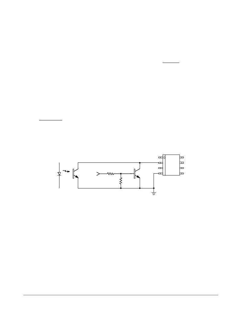
�Non--Latching� Shutdown�
�In� some� cases,� it� might� be� desirable� to� shut� off� the� device�
�temporarily� and� authorize� its� restart� once� the� control� signal�
�has� disappeared.� This� option� can� easily� be� accomplished�
�through� a� single� NPN� bipolar� transistor� wired� between� FB�
�and� ground.� By� pulling� FB� pin� voltage� below� the� V� SKIP�
�level,� the� output� pulses� are� disabled� as� long� as� FB� pin�
�voltage� is� pulled� below� the� skip� mode� threshold� voltage.� As�
�soon� as� FB� pin� is� released,� the� the� device� resumes� its� normal�
�operation� again.� Figure� 33� depicts� an� application� example.�
�1�
�2�
�8�
�7�
�ON/OFF�
�Q1�
�3�
�4�
�6�
�5�
�Figure� 33.� A� Method� to� Shut� Down� the� Device� Without� a� Definitive� Latchoff� State�
�Fault� Protection�
�In� applications� where� the� output� current� is� purposely� not�
�controlled� (e.g.� wall� adapters� delivering� raw� DC� level),� it� is�
�often� required� to� permanently� latchoff� the� power� supply� in�
�presence� of� a� fault.� This� fault� can� be� either� a� short--circuit� on�
�the� output� or� a� broken� optocoupler.� In� this� later� case,� it� is�
�important� to� quickly� react� in� order� to� avoid� a� lethal� output�
�voltage� runaway.� The� NCP1201� includes� a� circuitry� tailored�
�to� tackle� both� events.� A� short--circuit� forces� the� output�
�voltage� to� be� at� a� low� level,� preventing� a� bias� current� to�
�circulate� in� the� optocoupler� LED.� As� a� result,� the� FB� pin�
�level� is� pulled� up� to� 4.2� V,� as� internally� imposed� by� the� IC.�
�The� peak� current� set--point� goes� to� the� maximum� and� the�
�supply� delivers� a� rather� high� power� with� all� the� associated�
�effects.� However,� this� can� also� happen� in� case� of� feedback�
�loss,� e.g.� a� broken� optocoupler.� To� account� for� those�
�situations,� NCP1201� included� a� dedicated� overload�
�protection� circuitry.� Once� the� protection� activated,� the�
�circuitry� permanently� stops� the� pulses� while� the� V� CC� moves�
�between� 10--12� V� to� maintain� this� latchoff� state.� The� system�
�resets� when� the� user� purposely� cycles� the� V� CC� down� below�
�3.0� V,� e.g.� when� the� power� plug� is� removed� from� the� mains.�
�In� NCP1201,� the� controller� stops� all� output� pulses� as� soon�
�as� the� error� flag� is� asserted,� irrespective� to� the� V� CC� level.�
�However,� to� avoid� false� triggers� during� the� startup� sequence,�
�NCP1201� purposely� omits� the� very� first� V� CC� descent� from�
�12� to� 10� V.� The� error� circuitry� is� actually� armed� just� after� this�
�sequence,� e.g.� V� CC� crossing� 10� V.� Figure� 34� details� the�
�timing� sequence.� The� V� CC� capacitor� should� be� calculated�
�carefully� to� offer� a� sufficient� time� out� during� the� first� startup�
�V� CC� descent.�
�http://onsemi.com�
�14�
�相关PDF资料 |
PDF描述 |
|---|---|
| GBM10DTBT | CONN EDGECARD 20POS R/A .156 SLD |
| VE-25Y-CW-F3 | CONVERTER MOD DC/DC 3.3V 66W |
| REC3-2409SRW/H2/A | CONV DC/DC 3W 18-36VIN 09VOUT |
| EPM7064AETI100-7 | IC MAX 7000 CPLD 64 100-TQFP |
| RCB60DHAN-S621 | EDGECARD 120POS DIP R/A .050 SLD |
相关代理商/技术参数 |
参数描述 |
|---|---|
| NCP1201P100G | 功能描述:电流型 PWM 控制器 Current Mode PWM w/Fault Protection RoHS:否 制造商:Texas Instruments 开关频率:27 KHz 上升时间: 下降时间: 工作电源电压:6 V to 15 V 工作电源电流:1.5 mA 输出端数量:1 最大工作温度:+ 105 C 安装风格:SMD/SMT 封装 / 箱体:TSSOP-14 |
| NCP1201P60 | 功能描述:交流/直流开关转换器 Current Mode PWM RoHS:否 制造商:STMicroelectronics 输出电压:800 V 输入/电源电压(最大值):23.5 V 输入/电源电压(最小值):11.5 V 开关频率:115 kHz 电源电流:1.6 mA 工作温度范围:- 40 C to + 150 C 安装风格:SMD/SMT 封装 / 箱体:SSO-10 封装:Reel |
| NCP1201P60G | 功能描述:电流型 PWM 控制器 Current Mode PWM w/Fault Protection RoHS:否 制造商:Texas Instruments 开关频率:27 KHz 上升时间: 下降时间: 工作电源电压:6 V to 15 V 工作电源电流:1.5 mA 输出端数量:1 最大工作温度:+ 105 C 安装风格:SMD/SMT 封装 / 箱体:TSSOP-14 |
| NCP1203 | 制造商:ONSEMI 制造商全称:ON Semiconductor 功能描述:PWM Current-Mode Controller for Universal Off-Line Supplies Featuring Standby and Short Circuit |
| NCP1203/D | 制造商:未知厂家 制造商全称:未知厂家 功能描述:PWM Current-Mode Controller for Universal Off-Line Supplies Featuring Standby and Short Circuit Protection |
发布紧急采购,3分钟左右您将得到回复。