- 您现在的位置:买卖IC网 > Datasheet目录996 > NCP1216AFORWGEVB (ON Semiconductor)BOARD EVAL NCP1216A 35W Datasheet资料下载
参数资料
| 型号: | NCP1216AFORWGEVB |
| 厂商: | ON Semiconductor |
| 文件页数: | 11/18页 |
| 文件大小: | 0K |
| 描述: | BOARD EVAL NCP1216A 35W |
| 设计资源: | NCP1216AFORWGEVB Schematic NCP1216AFORWGEVB Gerber Files NCP1216AFORWGEVB Bill of Materials |
| 标准包装: | 1 |
| 系列: | * |
�� �
�
�NCP1216,� NCP1216A�
�the� nominal� switching� frequency� whose� sweep� is�
�synchronized� with� the� V� CC� ripple.� For� instance,� with� a� 2.2� V�
�peak� ?� to� ?� peak� ripple,� the� NCP1216P065� frequency� will�
�equal� 65� kHz� in� the� middle� of� the� ripple� and� will� increase� as�
�V� CC� rises� or� decrease� as� V� CC� ramps� down.� Figure� 20�
�portrays� the� behavior� we� have� adopted:�
�To� better� understand� how� this� skip� cycle� mode� takes� place,�
�a� look� at� the� operation� mode� versus� the� FB� level�
�immediately� gives� the� necessary� insight:�
�FB�
�VCC� OFF�
�V� CC� Ripple�
�65� kHz�
�68� kHz�
�Normal� Current� Mode� Operation�
�4.2� V,� F� B� Pin� Open�
�3.2� V,� Upper�
�Dynamic� Range�
�1V�
�Skip� Cycle� Operation�
�I� pMIN� =� 333� mV� /� R� sense�
�62� kHz�
�VCC� ON�
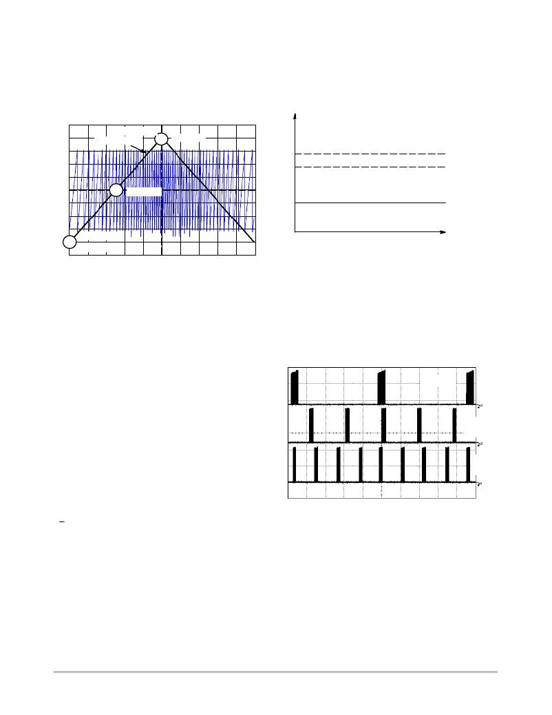
�Figure� 20.� V� CC� Ripple� is� Used� to� Introduce� a�
�Frequency� Jittering� on� the� Internal� Oscillator�
�Sawtooth�
�Skipping� Cycle� Mode�
�The� NCP1216� automatically� skips� switching� cycles� when�
�the� output� power� demand� drops� below� a� given� level.� This� is�
�accomplished� by� monitoring� the� FB� pin.� In� normal�
�operation,� pin� 2� imposes� a� peak� current� accordingly� to� the�
�load� value.� If� the� load� demand� decreases,� the� internal� loop�
�asks� for� less� peak� current.� When� this� setpoint� reaches� a�
�determined� level,� the� IC� prevents� the� current� from�
�decreasing� further� down� and� starts� to� blank� the� output�
�pulses:� the� IC� enters� the� so� ?� called� skip� cycle� mode,� also�
�named� controlled� burst� operation.� The� power� transfer� now�
�depends� upon� the� width� of� the� pulse� bunches� (Figure� 22).�
�Suppose� we� have� the� following� component� values:�
�L� p� ,� primary� inductance� =� 350� m� H�
�F� sw� ,� switching� frequency� =� 65� kHz�
�I� p� skip� =� 600� mA� (or� 333� mV� /� R� sense� )�
�The� theoretical� power� transfer� is� therefore:�
�Figure� 21.�
�When� FB� is� above� the� skip� cycle� threshold� (1.0� V� by�
�default),� the� peak� current� cannot� exceed� 1.0� V/R� sense� .� When�
�the� IC� enters� the� skip� cycle� mode,� the� peak� current� cannot� go�
�below� V� pin1� /� 3.3.� The� user� still� has� the� flexibility� to� alter� this�
�1.0� V� by� either� shunting� pin� 1� to� ground� through� a� resistor�
�or� raising� it� through� a� resistor� up� to� the� desired� level.�
�Grounding� pin� 1� permanently� invalidates� the� skip� cycle�
�operation.�
�Power P1�
�Power�
�P2�
�Power�
�P3�
�1�
�2�
�Lp�
�Ip2�
�Fsw� +� 4� W.�
�(eq.� 8)�
�Figure� 22.� Output� Pulses� at� Various� Power� Levels�
�(X� =� 5� m� s/div)� P1� <� P2� <� P3�
�If� this� IC� enters� skip� cycle� mode� with� a� bunch� length� of�
�10� ms� over� a� recurrent� period� of� 100� ms,� then� the� total� power�
�transfer� is:�
�4�
�0.1� +� 400� mW.�
�(eq.� 9)�
�http://onsemi.com�
�11�
�相关PDF资料 |
PDF描述 |
|---|---|
| NCP1351LEDGEVB | EVAL BOARD FOR NCP1351LEDG |
| NCP3065BBGEVB | BOARD EVAL NCP3065 MR16 BOOST |
| NCP3066SCBCKGEVB | EVAL BOARD FOR NCP3066SCBCKG |
| NCP5005GEVB | EVAL BOARD FOR NCP5005G |
| NCP5006EVB | EVAL BOARD FOR NCP5006 |
相关代理商/技术参数 |
参数描述 |
|---|---|
| NCP1216AP100 | 功能描述:开关变换器、稳压器与控制器 Current Mode PWM RoHS:否 制造商:Texas Instruments 输出电压:1.2 V to 10 V 输出电流:300 mA 输出功率: 输入电压:3 V to 17 V 开关频率:1 MHz 工作温度范围: 安装风格:SMD/SMT 封装 / 箱体:WSON-8 封装:Reel |
| NCP1216AP100G | 功能描述:电流型 PWM 控制器 Current Mode PWM w/50% Duty Cycle Max RoHS:否 制造商:Texas Instruments 开关频率:27 KHz 上升时间: 下降时间: 工作电源电压:6 V to 15 V 工作电源电流:1.5 mA 输出端数量:1 最大工作温度:+ 105 C 安装风格:SMD/SMT 封装 / 箱体:TSSOP-14 |
| NCP1216AP133 | 功能描述:电流型 PWM 控制器 Current Mode PWM RoHS:否 制造商:Texas Instruments 开关频率:27 KHz 上升时间: 下降时间: 工作电源电压:6 V to 15 V 工作电源电流:1.5 mA 输出端数量:1 最大工作温度:+ 105 C 安装风格:SMD/SMT 封装 / 箱体:TSSOP-14 |
| NCP1216AP133G | 功能描述:电流型 PWM 控制器 Current Mode PWM w/50% Duty Cycle Max RoHS:否 制造商:Texas Instruments 开关频率:27 KHz 上升时间: 下降时间: 工作电源电压:6 V to 15 V 工作电源电流:1.5 mA 输出端数量:1 最大工作温度:+ 105 C 安装风格:SMD/SMT 封装 / 箱体:TSSOP-14 |
| NCP1216AP65 | 功能描述:电流型 PWM 控制器 Current Mode PWM RoHS:否 制造商:Texas Instruments 开关频率:27 KHz 上升时间: 下降时间: 工作电源电压:6 V to 15 V 工作电源电流:1.5 mA 输出端数量:1 最大工作温度:+ 105 C 安装风格:SMD/SMT 封装 / 箱体:TSSOP-14 |
发布紧急采购,3分钟左右您将得到回复。