- 您现在的位置:买卖IC网 > PDF目录19659 > NCP1216AP133G (ON Semiconductor)IC CTRLR PWM CM OTP HV 8DIP PDF资料下载
参数资料
| 型号: | NCP1216AP133G |
| 厂商: | ON Semiconductor |
| 文件页数: | 10/18页 |
| 文件大小: | 0K |
| 描述: | IC CTRLR PWM CM OTP HV 8DIP |
| 标准包装: | 50 |
| 输出隔离: | 隔离 |
| 频率范围: | 120kHz ~ 146kHz |
| 输入电压: | 11 V ~ 16 V |
| 工作温度: | 0°C ~ 125°C |
| 封装/外壳: | 8-DIP(0.300",7.62mm),7 引线 |
| 供应商设备封装: | 7-PDIP |
| 包装: | 管件 |
�� �
�
�NCP1216,� NCP1216A�
�Dynamic� Self� ?� Supply�
�The� DSS� principle� is� based� on� the� charge/discharge� of� the�
�V� CC� bulk� capacitor� from� a� low� level� up� to� a� higher� level.� We�
�can� easily� describe� the� current� source� operation� with� a� bunch�
�of� simple� logical� equations:�
�POWER� ?� ON:� If� V� CC� <� VCC� OFF� then� the� Current� Source�
�is� ON,� no� output� pulses�
�If� V� CC� decreasing� >� VCC� ON� then� the� Current� Source� is�
�OFF,� output� is� pulsing�
�If� V� CC� increasing� <� VCC� OFF� then� the� Current� Source� is�
�ON,� output� is� pulsing�
�Typical� values� are:� VCC� OFF� =� 12.2� V,� VCC� ON� =� 10� V�
�To� better� understand� the� operational� principle,� Figure� 18�
�Application� note� AND8069/D� details� tricks� to� widen� the�
�NCP1216� driving� implementation,� in� particular� for� large� Q� g�
�MOSFETs.� This� document� can� be� downloaded� at�
�www.onsemi.com/pub/Collateral/AND8069� ?� D.PDF.�
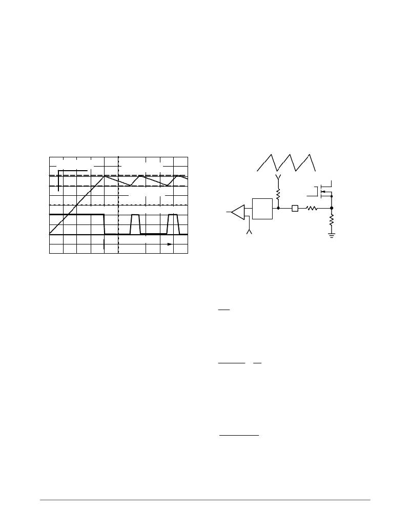
�Ramp� Compensation�
�Ramp� compensation� is� a� known� mean� to� cure�
�sub� ?� harmonic� oscillations.� These� oscillations� take� place� at�
�half� the� switching� frequency� and� occur� only� during�
�Continuous� Conduction� Mode� (CCM)� with� a� duty� ?� cycle�
�greater� than� 50%.� To� lower� the� current� loop� gain,� one� usually�
�injects� between� 50%� and� 100%� of� the� inductor� down� ?� slope.�
�Figure� 19� depicts� how� internally� the� ramp� is� generated:�
�offers� the� necessary� light:�
�V� ripple� = 2.2 V�
�VCC� OFF� = 12.2 V�
�VCC� ON� = 10 V�
�DC� max� =� 75� °� C�
�2.9V�
�0V�
�ON, I = 8 mA�
�OFF,� I� =� 0� mA�
�L.E.B�
�19� k�
�CS�
�R� comp�
�R� sense�
�Itotal� [� Fsw� Qg� )� ICC1.�
�Itotal� Vpin8.�
�65� kHz� +� 251� mV� m� s� ramp.�
�2.9�
�0.75�
�Vout� )� Vf� Np�
�+� 371� mA� m� s� or37� mV� m� s�
�19� k� divratio�
�+� 2.37� k� W�
�Output Pulse�
�10� 30� 50� 70� 90�
�Figure� 18.� The� Charge/Discharge� Cycle� Over� a�
�10� m� F� V� CC� Capacitor�
�The� DSS� behavior� actually� depends� on� the� internal� IC�
�consumption� and� the� MOSFET’s� gate� charge� Q� g� .� If� we�
�select� a� 600� V� 10� A� MOSFET� featuring� a� 30� nC� Q� g� ,� then� we�
�can� compute� the� resulting� average� consumption� supported�
�by� the� DSS� which� is:�
�(eq.� 1)�
�The� total� IC� heat� dissipation� incurred� by� the� DSS� only� is�
�given� by:�
�(eq.� 2)�
�Suppose� that� we� select� the� NCP1216P065� with� the� above�
�MOSFET,� the� total� current� is�
�(30� n� 65� k)� )� 900� m� +� 2.9� mA.� (eq.� 3)�
�Supplied� from� a� 350� VDC� rail� (250� VAC),� the� heat�
�dissipated� by� the� circuit� would� then� be:�
�350� V� 2.9� mA� +� 1� W� (eq.� 4)�
�As� you� can� see,� it� exists� a� tradeoff� where� the� dissipation�
�capability� of� the� NCP1216� fixes� the� maximum� Q� g� that� the�
�circuit� can� drive,� keeping� its� dissipation� below� a� given�
�target.� Please� see� the� “Power� Dissipation”� section� for� a�
�complete� design� example� and� discover� how� a� resistor� can�
�help� to� heal� the� NCP1216� heat� equation.�
�From� Set� ?� point�
�Figure� 19.� Inserting� a� Resistor� in� Series� with� the�
�Current� Sense� Information� brings� Ramp�
�Compensation�
�In� the� NCP1216,� the� ramp� features� a� swing� of� 2.9� V� with�
�a� Duty� cycle� max� at� 75%.� Over� a� 65� kHz� frequency,� it�
�corresponds� to� a�
�(eq.� 5)�
�In� our� FLYBACK� design,� let’s� suppose� that� our� primary�
�inductance� L� p� is� 350� m� H,� delivering� 12� V� with� a� Np� :� Ns�
�ratio� of� 1:0.1.� The� OFF� time� primary� current� slope� is� thus�
�given� by:�
�(eq.� 6)�
�Lp� Ns�
�when� projected� over� an� R� sense� of� 0.1� W� ,� for� instance.� If� we�
�select� 75%� of� the� down� ?� slope� as� the� required� amount� of�
�ramp� compensation,� then� we� shall� inject� 27� mV/� m� s.� Our�
�internal� compensation� being� of� 251� mV/� m� s,� the� divider� ratio�
�(divratio)� between� R� comp� and� the� 19� k� W� is� 0.107.� A� few� lines�
�of� algebra� to� determine� R� comp� :�
�(eq.� 7)�
�1� *� divratio�
�Frequency� Jittering�
�Frequency� jittering� is� a� method� used� to� soften� the� EMI�
�signature� by� spreading� the� energy� in� the� vicinity� of� the� main�
�switching� component.� NCP1216� offers� a� $� 4%� deviation� of�
�http://onsemi.com�
�10�
�相关PDF资料 |
PDF描述 |
|---|---|
| TAJT225M025RNJ | CAP TANT 2.2UF 25V 20% 1210 |
| VE-B0N-CY-F3 | CONVERTER MOD DC/DC 18.5V 50W |
| VE-B0L-CY-F1 | CONVERTER MOD DC/DC 28V 50W |
| NCP1217P100G | IC CTRLR PWM CM OVP HV 8DIP |
| TAP335M035GSB | CAP TANT 3.3UF 35V 20% RADIAL |
相关代理商/技术参数 |
参数描述 |
|---|---|
| NCP1216AP65 | 功能描述:电流型 PWM 控制器 Current Mode PWM RoHS:否 制造商:Texas Instruments 开关频率:27 KHz 上升时间: 下降时间: 工作电源电压:6 V to 15 V 工作电源电流:1.5 mA 输出端数量:1 最大工作温度:+ 105 C 安装风格:SMD/SMT 封装 / 箱体:TSSOP-14 |
| NCP1216AP65G | 功能描述:电流型 PWM 控制器 Current Mode PWM w/50% Duty Cycle Max RoHS:否 制造商:Texas Instruments 开关频率:27 KHz 上升时间: 下降时间: 工作电源电压:6 V to 15 V 工作电源电流:1.5 mA 输出端数量:1 最大工作温度:+ 105 C 安装风格:SMD/SMT 封装 / 箱体:TSSOP-14 |
| NCP1216D100 | 制造商:ONSEMI 制造商全称:ON Semiconductor 功能描述:PWM Current-Mode Controller for High-Power Universal Off-Line Supplies |
| NCP1216D100R2 | 功能描述:电流型 PWM 控制器 Current Mode PWM RoHS:否 制造商:Texas Instruments 开关频率:27 KHz 上升时间: 下降时间: 工作电源电压:6 V to 15 V 工作电源电流:1.5 mA 输出端数量:1 最大工作温度:+ 105 C 安装风格:SMD/SMT 封装 / 箱体:TSSOP-14 |
| NCP1216D100R2G | 功能描述:电流型 PWM 控制器 Current Mode PWM RoHS:否 制造商:Texas Instruments 开关频率:27 KHz 上升时间: 下降时间: 工作电源电压:6 V to 15 V 工作电源电流:1.5 mA 输出端数量:1 最大工作温度:+ 105 C 安装风格:SMD/SMT 封装 / 箱体:TSSOP-14 |
发布紧急采购,3分钟左右您将得到回复。