- 您现在的位置:买卖IC网 > PDF目录19523 > NCP1230D133R2 (ON Semiconductor)IC CTRLR PWM SMPS OVP OCP 8SOIC PDF资料下载
参数资料
| 型号: | NCP1230D133R2 |
| 厂商: | ON Semiconductor |
| 文件页数: | 16/21页 |
| 文件大小: | 0K |
| 描述: | IC CTRLR PWM SMPS OVP OCP 8SOIC |
| 产品变化通告: | Product Obsolescence 11/Feb/2009 |
| 标准包装: | 2,500 |
| 输出隔离: | 隔离 |
| 频率范围: | 133kHz |
| 输入电压: | 8.4 V ~ 18 V |
| 工作温度: | -40°C ~ 125°C |
| 封装/外壳: | 8-SOIC(0.154",3.90mm 宽) |
| 供应商设备封装: | 8-SOICN |
| 包装: | 带卷 (TR) |
�� �
�
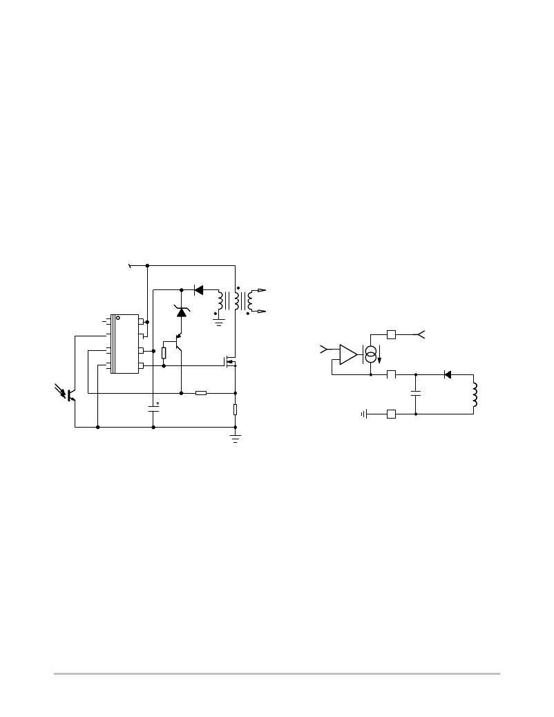
�NCP1230�
�Current� Sense� Input� Pin� Latch� ?� Off�
�The� NCP1230� features� a� fast� comparator� (Figure� 34)� that�
�monitors� the� current� sense� pin� during� the� controller� off� time.�
�If� for� any� reason� the� voltage� on� pin� 3� increases� above� 3.0� V,�
�the� NCP1230� immediately� stops� the� PWM� drive� pulses� and�
�permanently� stays� latched� off� until� the� bias� supply� to� the�
�NCP1230� is� cycled� down� (Vcc� must� drop� below� 4.0� V,� e.g.�
�when� the� user� unplugs� the� converter� from� the� mains).� This�
�offers� the� designer� the� flexibility� to� implement� an� externally�
�shutdown� circuit� (for� example� for� overvoltage� or�
�overtemperature� conditions).� When� the� controller� is� latched�
�off� through� pin� 3� (current� sense),� SW1� opens� and� shuts� off�
�PFC_Vcc� output.�
�Figure� 37� shows� how� to� implement� the� external� latch� via�
�a� Zener� diode� and� a� simple� PNP� transistor.� The� PNP� actually�
�samples� the� Zener� voltage� during� the� OFF� time� only,� hence�
�leaving� the� CS� information� un� ?� altered� during� the� ON� time.�
�Various� component� arrangements� can� be� made,� e.g.� adding�
�a� NTC� device� for� the� Over� Temperature� Protection� (OTP).�
�HV�
�Vz�
�Vccoff� (12.6� V� typically),� the� current� source� is� turned� off�
�reducing� the� amount� of� power� being� dissipated� in� the� chip.�
�The� NCP1230� then� turns� on� the� drive� output� to� the� external�
�MOSFET� in� an� attempt� to� increase� the� output� voltage� and�
�charge� up� the� Vcc� capacitor� through� the� Vaux� winding� in� the�
�transformer.�
�During� the� startup� sequence,� the� controller� pushes� for� the�
�maximum� peak� current,� which� is� reached� after� the� 2.5� ms�
�soft� ?� start� period.� As� soon� as� the� maximum� peak� set� point� is�
�reached,� the� internal� 1.0� V� Zener� diode� actively� limits� the�
�current� amplitude� to� 1.0� V/Rsense� and� asserts� an� error� flag�
�indicating� that� a� maximum� current� condition� is� being�
�observed.� In� this� mode,� the� controller� must� determine� if� it� is�
�a� normal� startup� period� (or� transient� load)� or� is� the� controller�
�is� facing� a� fault� condition.� To� determine� the� difference�
�between� a� normal� startup� sequence,� and� a� fault� condition,� the�
�error� flag� is� asserted,� and� the� 125� ms� timer� starts� to� count�
�down.� If� the� error� flag� drops� prior� to� the� 125� ms� time� ?� out�
�period,� the� controller� resets� the� timer� and� determines� that� it�
�was� a� normal� startup� sequence� and� enables� the� low�
�impedance� switch� (SW1),� enabling� the� PFC_Vcc� output.�
�If� at� the� end� of� the� 125� ms� period� the� error� flag� is� still�
�asserted,� then� the� controller� assumes� that� it� is� a� fault�
�condition� and� the� PWM� controller� enters� the� skip� mode� and�
�does� not� enable� the� PFC_Vcc� output.�
�1�
�8�
�2�
�7�
�8�
�HV�
�3�
�4�
�6�
�5�
�1k�
�12.6� V/�
�5.6� V�
�+�
�?�
�3.2� mA� or� 0�
�6�
�CVcc�
�Ramp�
�4�
�Figure� 38.�
�CVcc�
�Aux�
�Figure� 37.�
�Connecting� the� PNP� to� the� drive� only� activates� the� offset�
�generation� during� Toff.� Here� is� a� solution� monitoring� the�
�auziliary� Vcc� rail.�
�Drive� Output�
�The� NCP1230� provides� a� Drive� Output� which� can� be�
�connected� through� a� current� limiting� resistor� to� the� gate� of�
�a� MOSFET.� The� Driver� output� is� capable� of� delivering� drive�
�pulses� with� a� rise� time� of� 40� ns,� and� a� fall� time� of� 15� ns�
�through� its� internal� source� and� sink� resistance� of� 12.3� ohms�
�(typical),� measured� with� a� 1.0� nF� capacitive� load.�
�Startup� Sequence�
�The� NCP1230� has� an� internal� High� Voltage� Startup�
�Circuit� (Pin� 8)� which� is� connected� to� the� high� voltage� DC�
�bus� (Refer� to� Figure� 36).� When� power� is� applied� to� the� bus,�
�the� NCP1230� internal� current� source� (typically� 3.2� mA)� is�
�biased� and� charges� up� the� external� Vcc� capacitor� on� pin� 6,�
�refer� to� Figure� 38.� When� the� voltage� on� pin� 6� (Vcc)� reaches�
�ON� Semiconductor� recommends� that� the� Vcc� capacitor� be� at�
�least� 47� m� F� to� be� sure� that� the� Vcc� supply� voltage� does� not� drop�
�below� Vccmin� (7.7� V� typical)� during� standby� power� mode� and�
�unusual� fault� conditions.�
�Soft� ?� Start�
�The� NCP1230� features� an� internal� 2.5� ms� soft� ?� start�
�circuit.� As� soon� as� Vcc� reaches� a� nominal� 12.6� V,� the�
�soft� ?� start� circuit� is� activated.� The� soft� ?� start� circuit� output�
�controls� a� reference� on� the� minus� (� ?� )� input� to� an� amplifier�
�(refer� to� Figure� 39),� the� positive� (+)� input� to� the� amplifier� is�
�the� feedback� input� (divided� by� 3).� The� output� of� the�
�amplifier� drives� a� FET� which� clamps� the� feedback� signal.� As�
�the� soft� ?� start� circuit� output� ramps� up,� it� allow� the� feedback�
�pin� input� to� the� PWM� comparator� to� gradually� increased�
�from� near� zero� up� to� the� maximum� clamping� level� of� 1.0�
�V/Rsense.� This� occurs� over� the� entire� 2.5� ms� soft� ?� start�
�period� until� the� supply� enters� regulation.� The� soft� ?� start� is�
�also� activated� every� time� a� restart� is� attempted.� Figure� 40�
�shows� a� typical� soft� ?� start� up� sequence.�
�http://onsemi.com�
�16�
�相关PDF资料 |
PDF描述 |
|---|---|
| MCP98242T-CE/MNY | IC TEMP SENSOR 2WIRE 8-TDFN |
| GMA50DTKI-S288 | CONN EDGECARD 100POS .125 EXTEND |
| EBM06DRXN | CONN EDGECARD 12POS DIP .156 SLD |
| MINT1275A5614K01 | POWER SUPPLY MED 275W 56V |
| NMV0512SAC | CONV DC/DC 1W 5VIN 12VOUT SIP |
相关代理商/技术参数 |
参数描述 |
|---|---|
| NCP1230D133R2G | 功能描述:电流型 PWM 控制器 Low Standby Power High Performance PWM RoHS:否 制造商:Texas Instruments 开关频率:27 KHz 上升时间: 下降时间: 工作电源电压:6 V to 15 V 工作电源电流:1.5 mA 输出端数量:1 最大工作温度:+ 105 C 安装风格:SMD/SMT 封装 / 箱体:TSSOP-14 |
| NCP1230D165R2G | 功能描述:交流/直流开关转换器 ANA PWM CURRENT MODE CONT RoHS:否 制造商:STMicroelectronics 输出电压:800 V 输入/电源电压(最大值):23.5 V 输入/电源电压(最小值):11.5 V 开关频率:115 kHz 电源电流:1.6 mA 工作温度范围:- 40 C to + 150 C 安装风格:SMD/SMT 封装 / 箱体:SSO-10 封装:Reel |
| NCP1230D65R2 | 功能描述:电流型 PWM 控制器 Low Standby Power RoHS:否 制造商:Texas Instruments 开关频率:27 KHz 上升时间: 下降时间: 工作电源电压:6 V to 15 V 工作电源电流:1.5 mA 输出端数量:1 最大工作温度:+ 105 C 安装风格:SMD/SMT 封装 / 箱体:TSSOP-14 |
| NCP1230D65R2G | 功能描述:电流型 PWM 控制器 Low Standby Power High Performance PWM RoHS:否 制造商:Texas Instruments 开关频率:27 KHz 上升时间: 下降时间: 工作电源电压:6 V to 15 V 工作电源电流:1.5 mA 输出端数量:1 最大工作温度:+ 105 C 安装风格:SMD/SMT 封装 / 箱体:TSSOP-14 |
| NCP1230GEVB | 功能描述:电源管理IC开发工具 ANA NCP1230 EVAL BOARD RoHS:否 制造商:Maxim Integrated 产品:Evaluation Kits 类型:Battery Management 工具用于评估:MAX17710GB 输入电压: 输出电压:1.8 V |
发布紧急采购,3分钟左右您将得到回复。