- 您现在的位置:买卖IC网 > PDF目录15495 > NCP1395APG (ON Semiconductor)IC REG CTRLR PWM VM 16-DIP PDF资料下载
参数资料
| 型号: | NCP1395APG |
| 厂商: | ON Semiconductor |
| 文件页数: | 16/27页 |
| 文件大小: | 0K |
| 描述: | IC REG CTRLR PWM VM 16-DIP |
| 标准包装: | 25 |
| PWM 型: | 电压模式 |
| 输出数: | 2 |
| 频率 - 最大: | 1.11MHz |
| 占空比: | 52% |
| 电源电压: | 9.3 V ~ 20 V |
| 降压: | 无 |
| 升压: | 无 |
| 回扫: | 无 |
| 反相: | 无 |
| 倍增器: | 无 |
| 除法器: | 无 |
| Cuk: | 无 |
| 隔离: | 无 |
| 工作温度: | -40°C ~ 125°C |
| 封装/外壳: | 16-DIP(0.300",7.62mm) |
| 包装: | 管件 |
| 其它名称: | NCP1395APG-ND NCP1395APGOS |
第1页第2页第3页第4页第5页第6页第7页第8页第9页第10页第11页第12页第13页第14页第15页当前第16页第17页第18页第19页第20页第21页第22页第23页第24页第25页第26页第27页
�� �
�
�NCP1395A/B�
�The� designer� needs� to� program� the� maximum� switching�
�frequency� and� the� minimum� switching� frequency.� In� LLC�
�configurations,� for� circuits� working� above� the� resonant�
�frequency,� a� high� precision� is� required� on� the� minimum�
�frequency,� hence� the� "� 3%� specification.� This� minimum�
�switching� frequency� is� actually� reached� when� no� feedback�
�Figures� 35� and� 36� portray� the� frequency� evolution�
�depending� on� the� feedback� pin� voltage� level� in� a� different�
�frequency� clamp� combination.�
�F� A&B�
�closes� the� loop.� It� can� happen� during� the� startup� sequence,�
�a� strong� output� transient� loading� or� in� a� short� ?� circuit�
�Fmax�
�No� variations�
�1� MHz�
�condition.� By� installing� a� resistor� from� pin� 1� to� AGND,� the�
�minimum� frequency� is� set.� Using� the� same� philosophy,�
�wiring� a� resistor� from� pin� 2� to� AGND� will� set� the� maximum�
�frequency� excursion.� To� improve� the� circuit� protection�
�D� Fsw� =� 950� kHz�
�features,� we� have� purposely� created� a� dead� zone,� where� the�
�feedback� loop� has� no� action.� This� is� typically� below� 1.3� V.�
�Fmin�
�50� kHz�
�6V�
�1.3� V� D�
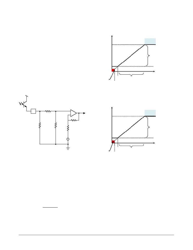
�Figure� 34� details� the� arrangement� where� the� internal�
�voltage� (that� drives� the� VCO)� varies� between� 0� and� 3.6� V.�
�However,� to� create� this� swing,� the� feedback� pin� (to� which�
�the� optocoupler� emitter� connects),� will� need� to� swing�
�typically� between� 1.3� V� and� 6.0� V.�
�V� CC�
�VFB�
�Fault�
�area� VFB� =� 4.7V�
�0.6� V�
�Figure� 35.� Maximal� default� excursion,� Rt� =� 120� k� W�
�on� pin� 1� and� Rfmax� =� 35� k� W� on� pin� 2.�
�VFB� =� 1.3� ?� 6� V�
�To� VCO�
�F� A&B�
�FB�
�+�
�?�
�0� to� 3.6� V�
�Fmax�
�No� variations�
�450� kHz�
�Rfb�
�D� Fsw� =� 300� kHz�
�+�
�1.3� V�
�Fmin�
�150� kHz�
�VFB�
�6V�
�1.3� V� D�
�slope� will� then� be�
�+� 202� kHz� V.�
�Figure� 34.� The� OPAMP� arrangement� limits� the� VCO�
�internal� modulation� signal� between� 0� and� 5.0� V.�
�This� technique� allows� us� to� detect� a� fault� on� the� converter�
�in� case� the� FB� pin� cannot� rise� above� 1.3� V� (to� actually� close�
�the� loop)� in� less� than� a� duration� imposed� by� the�
�programmable� timer.� Please� refer� to� the� fault� section� for�
�detailed� operation� of� this� mode.�
�As� shown� in� Figure� 34,� the� internal� dynamics� of� the�
�VCO� control� voltage� will� be� constrained� between� 0� V� and�
�3.6� V,� whereas� the� feedback� loop� will� drive� pin� 5� (FB)�
�between� 1.3� V� and� 6.0� V.� If� we� take� the� external� excursion�
�numbers,� 1.3� V� =� 50� kHz,� 6.0� V� =� 1.0� MHz,� then� the� VCO�
�1 Meg� ?� 50 k�
�4.7�
�Fault�
�area� VFB� =� 4.7� V�
�0.6� V�
�Figure� 36.� Here� a� different� minimum� frequency�
�was� programmed� as� well� as� a� different� maximum�
�frequency� excursion.�
�Please� note� that� the� previous� small� signal� VCO� slope� has�
�now� been� reduced� to� 300� k/5.0� =� 62.5� kHz/V.� This� offers�
�a� mean� to� magnify� the� feedback� excursion� on� systems�
�where� the� load� range� does� not� generate� a� wide� switching�
�frequency� excursion.� Due� to� this� option,� we� will� see� how�
�it� becomes� possible� to� observe� the� feedback� level� and�
�implement� skip� cycle� at� light� loads.� It� is� important� to� note�
�that� the� frequency� evolution� does� not� have� a� real� linear�
�relationship� with� the� feedback� voltage.� This� is� due� to� the�
�deadtime� presence� which� stays� constant� as� the� switching�
�period� changes.�
�http://onsemi.com�
�16�
�相关PDF资料 |
PDF描述 |
|---|---|
| 4302-223K | INDUCTOR TEMP STABLE 22UH SMD |
| 4302-183K | INDUCTOR TEMP STABLE 18UH SMD |
| 4302-153K | INDUCTOR TEMP STABLE 15UH SMD |
| 4302-123K | INDUCTOR TEMP STABLE 12UH SMD |
| 4302-103K | INDUCTOR TEMP STABLE 10UH SMD |
相关代理商/技术参数 |
参数描述 |
|---|---|
| NCP1395B | 制造商:ONSEMI 制造商全称:ON Semiconductor 功能描述:High Performance Resonant Mode Controller |
| NCP1395BDR2G | 功能描述:电压模式 PWM 控制器 PWM CONTROLLER RoHS:否 制造商:Texas Instruments 输出端数量:1 拓扑结构:Buck 输出电压:34 V 输出电流: 开关频率: 工作电源电压:4.5 V to 5.5 V 电源电流:600 uA 最大工作温度:+ 125 C 最小工作温度:- 40 C 封装 / 箱体:WSON-8 封装:Reel |
| NCP1395BPG | 功能描述:电压模式 PWM 控制器 PWM CONTROLLER RoHS:否 制造商:Texas Instruments 输出端数量:1 拓扑结构:Buck 输出电压:34 V 输出电流: 开关频率: 工作电源电压:4.5 V to 5.5 V 电源电流:600 uA 最大工作温度:+ 125 C 最小工作温度:- 40 C 封装 / 箱体:WSON-8 封装:Reel |
| NCP1395D | 制造商:ONSEMI 制造商全称:ON Semiconductor 功能描述:High Performance Resonant Mode Controller |
| NCP1395LLCGEVB | 功能描述:BOARD EVAL NCP1395 RoHS:是 类别:编程器,开发系统 >> 评估板 - DC/DC 与 AC/DC(离线)SMPS 系列:* 产品培训模块:Obsolescence Mitigation Program 标准包装:1 系列:True Shutdown™ 主要目的:DC/DC,步升 输出及类型:1,非隔离 功率 - 输出:- 输出电压:- 电流 - 输出:1A 输入电压:2.5 V ~ 5.5 V 稳压器拓扑结构:升压 频率 - 开关:3MHz 板类型:完全填充 已供物品:板 已用 IC / 零件:MAX8969 |
发布紧急采购,3分钟左右您将得到回复。