- 您现在的位置:买卖IC网 > PDF目录13323 > NCP1530DM27R2 (ON Semiconductor)IC REG BUCK 2.7V 0.6A MICRO8 PDF资料下载
参数资料
| 型号: | NCP1530DM27R2 |
| 厂商: | ON Semiconductor |
| 文件页数: | 13/16页 |
| 文件大小: | 0K |
| 描述: | IC REG BUCK 2.7V 0.6A MICRO8 |
| 产品变化通告: | LTB Notification 03/Jan/2008 |
| 标准包装: | 4,000 |
| 类型: | 降压(降压) |
| 输出类型: | 固定 |
| 输出数: | 1 |
| 输出电压: | 2.7V |
| 输入电压: | 3.7 V ~ 5.5 V |
| PWM 型: | 电流模式 |
| 频率 - 开关: | 600kHz |
| 电流 - 输出: | 600mA |
| 同步整流器: | 无 |
| 工作温度: | 0°C ~ 85°C |
| 安装类型: | 表面贴装 |
| 封装/外壳: | 8-TSSOP,8-MSOP(0.118",3.00mm 宽) |
| 包装: | 带卷 (TR) |
| 供应商设备封装: | Micro8? |
�� �
�
�NCP1530�
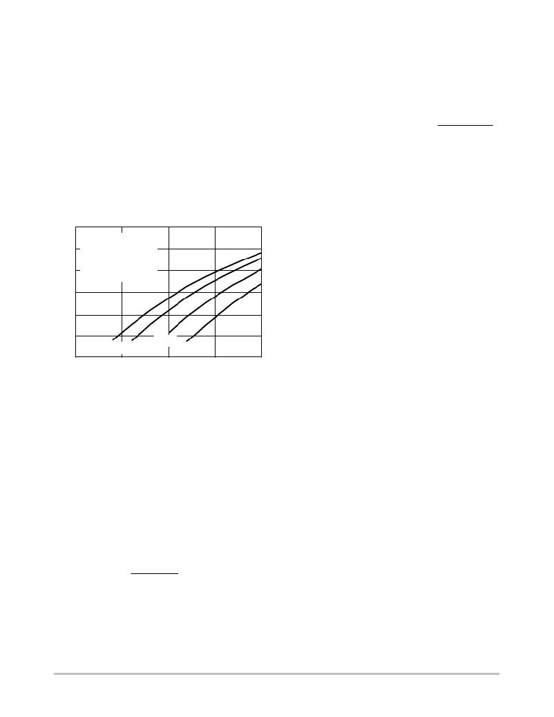
�For� ease� of� application,� the� previous� equation� was�
�plotted� in� Figure� 35� to� help� end� user� to� select� the� right�
�inductor� for� specific� application.� As� a� rule� of� thumb,� the�
�user� needs� to� be� aware� of� the� maximum� peak� inductor�
�current� and� should� be� designed� not� to� exceed� the� saturation�
�limit� of� the� inductor� selected.� Low� inductance� can� supply�
�Output� Capacitor� Selection�
�Selection� of� the� output� capacitor,� C� OUT� is� primarily�
�governed� by� the� required� effective� series� resistance� (ESR)�
�of� the� capacitor.� Typically,� once� the� ESR� requirement� is�
�met,� the� capacitance� will� be� adequate� for� filtering.� The�
�output� voltage� ripple,� V� RIPPLE� is� approximated� by,�
�higher� output� current,� but� suffers� higher� output� ripple� and�
�reduced� efficiency,� but� it� limits� the� output� current�
�VRIPPLE� [� IL_RIPPLE(P� *� P)�
�ESR� )�
�4�
�1�
�FOSCCOUT�
�capability.� On� the� other� hand,� high� inductance� can� improve�
�output� ripple� and� efficiency,� at� the� same� time,� it� also� limits�
�the� output� current� capability.� One� other� critical� parameter�
�of� the� inductor� is� its� DC� resistance.� This� resistance� can�
�introduce� unwanted� power� loss� and� hence� reduce� overall�
�efficiency.� The� basic� rule� is� selecting� an� inductor� with�
�lowest� DC� resistance� within� the� board� space� limitation.�
�Where� F� OSC� is� the� switching� frequency� and� ESR� is� the�
�effective� series� resistance� of� the� output� capacitor.�
�From� equation� in� above,� it� can� be� noted� that� the� output�
�voltage� ripple� is� contributed� to� by� two� parts.� For� most� of� the�
�cases,� the� major� contributor� is� the� capacitor� ’s� ESR.�
�Ordinary� aluminum?electrolytic� capacitors� have� high� ESR�
�and� should� be� avoided.� High� quality� Low� ESR�
�12�
�10�
�8.0�
�6.0�
�4.0�
�R� DS(ON)� =� 3.0� W�
�D1,� MBRM120ET3�
�C� IN� =� C� OUT� =� 22� m� F�
�I� OUT� =� 600� mA�
�I� L_RIPPLE(P?P)� =� 0.2� A�
�aluminum?electrolytic� capacitors� are� acceptable� and�
�relatively� inexpensive.� Low� ESR� tantalum� capacitors� are�
�another� alternative.� For� even� better� performance,� surface�
�mounted� ceramic� capacitors� can� be� used.� Ceramic�
�capacitors� have� lowest� ESR� among� all� choices.� The�
�NCP1530� is� internally� compensated� for� stable� operation�
�with� low� ESR� ceramic� capacitors.� However,� ordinary�
�multi?layer� ceramic� capacitors� have� poor� temperature� and�
�frequency� performance,� for� switching� applications,� so� only�
�high� quality,� grade� X5R� and� X7R� ceramic� capacitors� can�
�2.0�
�2.5� V�
�2.7� V�
�3.0� V�
�3.3� V�
�be� used.�
�PCB� Layout� Recommendations�
�0�
�3.0�
�3.5�
�4.0�
�4.5�
�5.0�
�Good� PCB� layout� plays� an� important� role� in� switching�
�mode� power� conversion.� Careful� PCB� layout� can� help� to�
�V� IN� ,� INPUT� VOLTAGE� (V)�
�Figure� 35.� Inductor� Selection� Chart�
�Flywheel� Diode� Selection�
�The� flywheel� diode� is� turned� on� and� carries� load� current�
�during� the� off� time.� At� high� input� voltages,� the� diode�
�conducts� most� of� the� time.� In� the� case� where� V� IN�
�approaches� V� OUT� ,� the� diode� conducts� only� a� small� fraction�
�of� the� cycle.� While� the� output� terminals� are� shorted,� the�
�diode� will� be� subject� to� its� highest� stress.� Under� this�
�condition,� the� diode� must� be� able� to� safely� handle� the� peak�
�current� circulating� in� the� loop.� So,� it� is� important� to� select�
�a� flywheel� diode� that� can� meet� the� diode� peak� current� and�
�average� power� dissipation� requirements.� Under� normal�
�conditions,� the� average� current� conducted� by� the� flywheel�
�diode� is� given� by,�
�minimize� ground� bounce,� EMI� noise� and� unwanted�
�feedbacks� that� can� affect� the� performance� of� the� converter.�
�Hints� suggested� below� can� be� used� as� a� guideline� in� most�
�situations.�
�Grounding�
�Star?ground� connection� should� be� used� to� connect� the�
�output� power� return� ground,� the� input� power� return� ground�
�and� the� device� power� ground� together� at� one� point.� All� high�
�current� running� paths� must� be� thick� enough� for� current�
�flowing� through� and� producing� insignificant� voltage� drop�
�along� the� path.�
�Components� Placement�
�Power� components,� i.e.� input� capacitor,� inductor� and�
�output� capacitor,� must� be� placed� as� close� together� as�
�possible.� All� connecting� traces� must� be� short,� direct� and�
�thick.� High� current� flowing� and� switching� paths� must� be�
�ID� +� IN�
�V� *� VOUT�
�VIN� )� VF�
�IOUT�
�kept� away� from� the� feedback� (V� OUT� ,� pin� 6)� terminal� to�
�avoid� unwanted� injection� of� noise� into� the� feedback� path.�
�Where� I� D� is� the� average� diode� current� and� V� F� is� the� forward�
�voltage� drop� of� the� diode.�
�A� low� forward� voltage� drop� and� fast� switching� diode�
�must� also� be� used� to� optimize� converter� efficiency.�
�Schottky� diodes� are� a� good� choice� for� low� forward� drop� and�
�fast� switching� times.�
�Feedback� Path�
�Feedback� of� the� output� voltage� must� be� a� separate� trace�
�separated� from� the� power� path.� The� output� voltage� sensing�
�trace� to� the� feedback� (V� OUT� ,� pin� 6)� pin� should� be� connected�
�to� the� output� voltage� directly� at� the� anode� of� the� output�
�capacitor.�
�http://onsemi.com�
�13�
�相关PDF资料 |
PDF描述 |
|---|---|
| XC6210B252MR-G | IC REG LDO 2.5V .7A SOT-25 |
| ABB30DHNN | CONN EDGECARD 60POS .050 DIP SLD |
| 500R07W471KV4T | CAP CER 470PF 50V 10% X7R 0402 |
| NCP1530DM25R2 | IC REG BUCK 2.5V 0.6A MICRO8 |
| SC5040F-471 | INDUCTOR SMD 470UH 2.2A 100KHZ |
相关代理商/技术参数 |
参数描述 |
|---|---|
| NCP1530DM27R2G | 功能描述:直流/直流开关转换器 600mA PWM/PFM Buck RoHS:否 制造商:STMicroelectronics 最大输入电压:4.5 V 开关频率:1.5 MHz 输出电压:4.6 V 输出电流:250 mA 输出端数量:2 最大工作温度:+ 85 C 安装风格:SMD/SMT |
| NCP1530DM30R2 | 功能描述:直流/直流开关转换器 600mA PWM/PFM Buck RoHS:否 制造商:STMicroelectronics 最大输入电压:4.5 V 开关频率:1.5 MHz 输出电压:4.6 V 输出电流:250 mA 输出端数量:2 最大工作温度:+ 85 C 安装风格:SMD/SMT |
| NCP1530DM30R2G | 功能描述:直流/直流开关转换器 600mA PWM/PFM Buck RoHS:否 制造商:STMicroelectronics 最大输入电压:4.5 V 开关频率:1.5 MHz 输出电压:4.6 V 输出电流:250 mA 输出端数量:2 最大工作温度:+ 85 C 安装风格:SMD/SMT |
| NCP1530DM33R2 | 功能描述:直流/直流开关转换器 600mA PWM/PFM Buck RoHS:否 制造商:STMicroelectronics 最大输入电压:4.5 V 开关频率:1.5 MHz 输出电压:4.6 V 输出电流:250 mA 输出端数量:2 最大工作温度:+ 85 C 安装风格:SMD/SMT |
| NCP1530DM33R2G | 功能描述:直流/直流开关转换器 600mA PWM/PFM Buck RoHS:否 制造商:STMicroelectronics 最大输入电压:4.5 V 开关频率:1.5 MHz 输出电压:4.6 V 输出电流:250 mA 输出端数量:2 最大工作温度:+ 85 C 安装风格:SMD/SMT |
发布紧急采购,3分钟左右您将得到回复。