- 您现在的位置:买卖IC网 > PDF目录13696 > NCP1546MNR2G (ON Semiconductor)IC REG BUCK 1.5A 18DFN PDF资料下载
参数资料
| 型号: | NCP1546MNR2G |
| 厂商: | ON Semiconductor |
| 文件页数: | 8/15页 |
| 文件大小: | 0K |
| 描述: | IC REG BUCK 1.5A 18DFN |
| 标准包装: | 1 |
| 类型: | 降压(降压) |
| 输出数: | 1 |
| 输入电压: | 4.5 V ~ 40 V |
| PWM 型: | 混合物 |
| 频率 - 开关: | 170kHz |
| 电流 - 输出: | 1.5A |
| 同步整流器: | 无 |
| 工作温度: | 0°C ~ 70°C |
| 安装类型: | 表面贴装 |
| 封装/外壳: | 18-VFDFN 裸露焊盘 |
| 包装: | 剪切带 (CT) |
| 供应商设备封装: | 18-DFN(5x6) |
| 其它名称: | NCP1546MNR2GOSCT |
�� �
�
�NCP1546�
�30�
�25�
�20�
�15�
�10�
�5�
�0�
�0�
�0.5� 1.0�
�1.5�
�SWITCHING� CURRENT� (A)�
�Figure� 9.� The� Boost� Pin� Current� Includes� 7.0� mA�
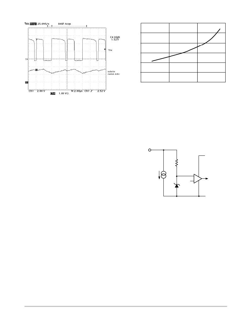
�Figure� 8.� The� Regulator� in� Current� Limit�
�BOOST� Pin�
�The� BOOST� pin� provides� base� driving� current� for� the�
�power� switch.� A� voltage� higher� than� V� IN� provides� required�
�headroom� to� turn� on� the� power� switch.� This� in� turn� reduces�
�IC� power� dissipation� and� improves� overall� system�
�efficiency.� The� BOOST� pin� can� be� connected� to� an� external�
�boost� ?� strapping� circuit� which� typically� uses� a� 0.1� m� F�
�capacitor� and� a� 1N914� or� 1N4148� diode,� as� shown� in� Figure�
�1.� When� the� power� switch� is� turned� on,� the� voltage� on� the�
�Pre� ?� Driver� Current� and� Base� Current� when� the�
�Switch� is� Turned� On.� The� Beta� Decline� of� the�
�Power� Switch� Further� Increases� the� Base�
�Current� at� High� Switching� Current�
�Shutdown�
�The� internal� power� switch� will� not� turn� on� until� the� V� IN�
�pin� rises� above� the� Startup� Voltage.� This� ensures� no�
�switching� will� occur� until� adequate� supply� voltage� is�
�provided� to� the� IC.� Refer� to� Figure� 10� for� the� SHDNB�
�(shutdown� ?� bar)� pin� input� circuit.�
�BOOST� pin� is� equal� to�
�VBOOST� +� VIN� )� VO� *� VF�
�where:�
�V� F� =� diode� forward� voltage.�
�The� anode� of� the� diode� can� be� connected� to� any� DC�
�voltage� as� well� as� the� regulated� output� voltage� (Figure� 1).�
�SHDNB�
�20k�
�±� 33%�
�-�
�V� IN�
�However,� the� maximum� voltage� on� the� BOOST� pin� shall� not�
�1.2V�
�+�
�exceed� 40� V.�
�As� shown� in� Figure� 9,� the� BOOST� pin� current� includes� a�
�constant� 7.0� mA� pre� ?� driver� current� and� base� current�
�proportional� to� switch� conducting� current.� A� detailed�
�discussion� of� this� current� is� conducted� in� Thermal�
�Consideration� section.� A� 0.1� m� F� capacitor� is� usually� adequate�
�for� maintaining� the� Boost� pin� voltage� during� the� on� time.�
�V� Z� =� 6V� to� 8V�
�GND�
�Figure� 10.�
�The� IC� enters� a� sleep� mode� when� the� SHDNB� pin� is� pulled�
�below� the� Shutdown� Threshold� Voltage.� In� sleep� mode,� the�
�power� switch� is� kept� open� and� the� supply� current� reduces� to�
�Shutdown� Quiescent� Current� (� 1� m� A� typically).� This� pin� has�
�an� internal� pull� ?� down� current.� When� not� in� use,� pull� this� pin�
�up� to� V� CC� with� a� resistor� (See� Figure� 1).� A� 100� k� W� pullup�
�resistor� will� ensure� safe� operation� from� below� 9� V� and�
�during� a� 40� V� load� dump� condition.�
�http://onsemi.com�
�8�
�相关PDF资料 |
PDF描述 |
|---|---|
| MAX6727AKARYD6+T | IC SUPERVISOR MPU SOT23-8 |
| VI-J5F-CZ-S | CONVERTER MOD DC/DC 72V 25W |
| MAX6727AKASDD1+T | IC SUPERVISOR MPU SOT23-8 |
| 80ZLH68MEFCTA8X16 | CAP ALUM 68UF 80V 20% RADIAL |
| VE-25B-EX-F1 | CONVERTER MOD DC/DC 95V 75W |
相关代理商/技术参数 |
参数描述 |
|---|---|
| NCP1547DG | 功能描述:直流/直流开关调节器 340 KHZ REGULATOR RoHS:否 制造商:International Rectifier 最大输入电压:21 V 开关频率:1.5 MHz 输出电压:0.5 V to 0.86 V 输出电流:4 A 输出端数量: 最大工作温度: 安装风格:SMD/SMT 封装 / 箱体:PQFN 4 x 5 |
| NCP1547DR2G | 功能描述:直流/直流开关调节器 340 KHZ REGULATOR RoHS:否 制造商:International Rectifier 最大输入电压:21 V 开关频率:1.5 MHz 输出电压:0.5 V to 0.86 V 输出电流:4 A 输出端数量: 最大工作温度: 安装风格:SMD/SMT 封装 / 箱体:PQFN 4 x 5 |
| NCP1547MNR2G | 功能描述:直流/直流开关调节器 340 KHZ RoHS:否 制造商:International Rectifier 最大输入电压:21 V 开关频率:1.5 MHz 输出电压:0.5 V to 0.86 V 输出电流:4 A 输出端数量: 最大工作温度: 安装风格:SMD/SMT 封装 / 箱体:PQFN 4 x 5 |
| NCP1550SN18T1 | 功能描述:直流/直流开关转换器 1.8V 2A Buck PWM/PFM RoHS:否 制造商:STMicroelectronics 最大输入电压:4.5 V 开关频率:1.5 MHz 输出电压:4.6 V 输出电流:250 mA 输出端数量:2 最大工作温度:+ 85 C 安装风格:SMD/SMT |
| NCP1550SN18T1G | 功能描述:直流/直流开关转换器 1.8V 2A Buck PWM/PFM w/Enable Soft Start RoHS:否 制造商:STMicroelectronics 最大输入电压:4.5 V 开关频率:1.5 MHz 输出电压:4.6 V 输出电流:250 mA 输出端数量:2 最大工作温度:+ 85 C 安装风格:SMD/SMT |
发布紧急采购,3分钟左右您将得到回复。