- 您现在的位置:买卖IC网 > PDF目录15088 > NCP1550SN30T1 (ON Semiconductor)IC REG CTRLR BUCK PWM VM 5TSOP PDF资料下载
参数资料
| 型号: | NCP1550SN30T1 |
| 厂商: | ON Semiconductor |
| 文件页数: | 14/17页 |
| 文件大小: | 0K |
| 描述: | IC REG CTRLR BUCK PWM VM 5TSOP |
| 产品变化通告: | LTB Notification 03/Jan/2008 |
| 标准包装: | 3,000 |
| PWM 型: | 电压模式 |
| 输出数: | 1 |
| 频率 - 最大: | 690kHz |
| 占空比: | 100% |
| 电源电压: | 2.45 V ~ 5.5 V |
| 降压: | 是 |
| 升压: | 无 |
| 回扫: | 无 |
| 反相: | 无 |
| 倍增器: | 无 |
| 除法器: | 无 |
| Cuk: | 无 |
| 隔离: | 无 |
| 工作温度: | -40°C ~ 85°C |
| 封装/外壳: | 6-TSOP(0.059",1.50mm 宽)5 引线 |
| 包装: | 带卷 (TR) |
| 其它名称: | NCP1550SN30T1OS |
�� �
�
�NCP1550�
�APPLICATIONS� INFORMATION�
�Inductor� Value� Calculation�
�Selecting� the� proper� inductance� is� a� trade?off� between�
�inductor’s� physical� size,� transient� respond� and� power�
�conversion� requirements.� Lower� value� inductor� saves� cost,�
�PC� board� space� and� providing� faster� transient� response,� but�
�result� in� higher� ripple� current� and� core� losses.� Considering� an�
�application� with� loading� current,� I� OUT� =� 0.5� A� and� the�
�inductor� ripple� current,� I� L?RIPPLE(P?P)� is� designed� to� be� less�
�than� 40%� of� the� load� current,� i.e.� 0.5� A� x� 40%� =� 0.2� A.�
�The� relationship� between� the� inductor� value� and� inductor�
�P?Channel� switch� duty� cycle.� At� high� input� voltages,� the�
�diode� conducts� most� of� the� time.� In� case� of� V� IN� approaches�
�V� OUT� ,� the� diode� conducts� only� a� small� fraction� of� the� cycle.�
�While� the� output� terminals� are� shorted,� the� diode� will� subject�
�to� its� highest� stress.� Under� this� condition,� the� diode� must� be�
�able� to� safely� handle� the� peak� current� circulating� in� the� loop.�
�So,� it� is� important� to� select� a� flywheel� diode� that� can� meet� the�
�diode� peak� current� and� average� power� dissipation�
�requirements.� Under� normal� conditions,� the� average� current�
�conducted� by� the� flywheel� diode� is� given� by:�
�L� +� ON�
�ID� +� VIN� *� VOUT� IOUT� (eq.� 2)�
�ripple� current� is� given� by,�
�T * (VIN� *� RDS(ON) IOUT� *� VOUT)�
�IL� *� RIPPLE(P� *� P)�
�(eq.� 1)�
�VIN� )� VF�
�Where� I� D� is� the� average� diode� current� and� V� F� is� the� forward�
�Where� R� DS(ON)� is� the� ON� resistance� of� the� external�
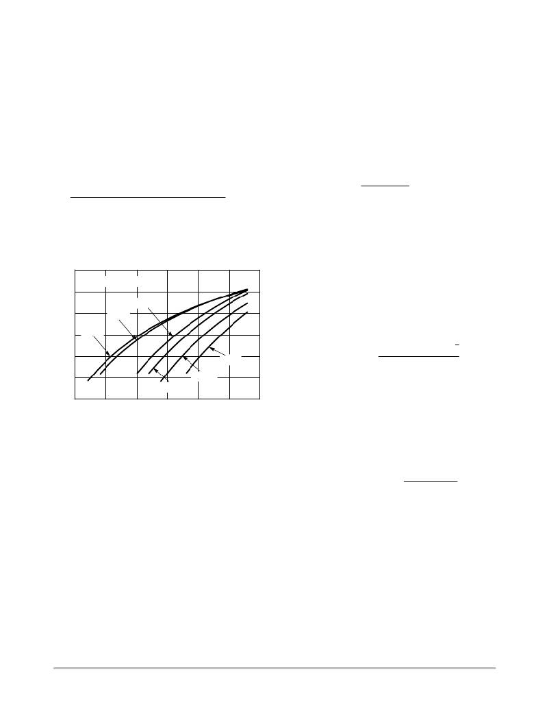
�P?channel� MOSFET.� Figure� 39� is� a� plot� for� recommended�
�inductance� against� nominal� input� voltage� for� different� output�
�options.�
�diode� voltage� drop.�
�A� fast� switching� diode� must� also� be� used� to� optimize�
�efficiency.� Schottky� diodes� are� a� good� choice� for� low� forward�
�drop� and� fast� switching� times.�
�12�
�10�
�8�
�6�
�R� DS(ON)� = 0.1� W�
�1.9� V�
�1.8� V�
�2.5� V�
�Input� and� Output� Capacitor� Selection� (C� IN� and� C� OUT� )�
�In� continuous� mode� operation,� the� source� current� of� the�
�P?Channel� MOSFET� is� a� square� wave� of� duty� cycle� (V� OUT� +�
�V� F� )/V� IN� .� To� prevent� large� input� voltage� transients,� a� low� ESR�
�input� capacitor� that� can� support� the� maximum� RMS� input�
�current� must� be� selected.� The� maximum� RMS� input� current,�
�I� RMS(MAX)� can� be� estimated� by� the� equation� in� below:�
�4�
�3.3 V�
�IRMS(MAX)� [� IOUT�
�1�
�VOUT(VIN� *� VOUT)� 2�
�VIN�
�(eq.� 3)�
�2�
�0�
�2.7� V�
�3.0� V�
�Above� estimation� has� a� maximum� value� at� V� IN� =� 2V� OUT� ,�
�where� I� RMS(MAX)� =� I� OUT� /2.� As� a� general� practice,� this� simple�
�worst?case� condition� is� used� for� design.�
�2.2�
�2.7�
�3.2�
�3.7�
�4.2�
�4.7�
�5.2�
�Selection� of� the� output� capacitor,� C� OUT� is� primarily�
�1�
�V� IN� ,� INPUT� VOLTAGE� OF� NCP1550� (V)�
�Figure� 39.� Inductor� Selection� Chart�
�P?Channel� Power� MOSFET� Selection�
�An� external� P?Channel� power� MOSFET� must� be� used� with�
�the� NCP1550.� The� key� selection� criteria� for� the� power�
�MOSFET� are� the� gate� threshold,� V� GS� ,� the� “ON”� resistance,�
�R� DS(ON)� and� its� total� gate� charge,� Q� T� .� For� low� input� voltage�
�operation,� we� need� to� select� a� low� gate� threshold� device� that�
�can� work� down� to� the� minimum� input� voltage� level.� R� DS(ON)�
�determines� the� conduction� losses� for� each� switching� cycle,�
�the� lower� the� ON� resistance,� the� higher� the� efficiency� can� be�
�achieved.� A� power� MOSFET� with� lower� gate� charge� can� give�
�lower� switching� losses� but� the� fast� transient� can� cause�
�unwanted� EMI� to� the� system.� Compromise� in� between� is�
�required� during� the� design� stage.� For� 1.0� A� and� 2.0� A� load�
�current,� NTGS3441T1� and� NTGS3443T1� are� tested� to� be�
�appropriate� for� most� applications.�
�governed� by� the� required� effective� series� resistance� (ESR)� of�
�the� capacitor.� Typically,� once� the� ESR� requirement� is� met,� the�
�capacitance� will� be� adequate� for� filtering.� The� output� voltage�
�ripple,� V� RIPPLE� is� approximated� by:�
�VRIPPLE� [� IL� *� RIPPLE(P� *� P)�
�(eq.� 4)�
�(ESR� )� )�
�4� FOSCCOUT�
�Where� F� OSC� is� the� switching� frequency� and� ESR� is� the�
�effective� series� resistance� of� the� output� capacitor.�
�From� equation� (4),� it� can� be� noted� that� the� output� voltage�
�ripple� contributed� by� two� parts.� For� most� of� the� case,� the�
�major� contributor� is� the� capacitor� ESR.� Ordinary�
�aluminum?electrolytic� capacitors� have� high� ESR� and� should�
�be� avoided.� Higher� quality� Low� ESR� aluminum?electrolytic�
�capacitors� are� acceptable� and� relatively� inexpensive.� For� even�
�better� performance,� Low� ESR� tantalum� capacitors� should� be�
�used.� Surface?mount� tantalum� capacitors� are� better� and�
�provide� neat� and� compact� solution� for� space� sensitive�
�applications.�
�Flywheel� Diode� Selection�
�The� flywheel� diode� is� turned� on� and� carries� load� current�
�during� the� off� time.� The� average� diode� current� depends� on� the�
�http://onsemi.com�
�14�
�相关PDF资料 |
PDF描述 |
|---|---|
| X4043M8IZ-2.7T1 | IC CPU SUPERV 4K EEPROM 8-MSOP |
| RCM28DRYI-S13 | CONN EDGECARD 56POS .156 EXTEND |
| X5043S8Z | IC CPU SUPERV 4K EEPROM 8-SOIC |
| X5043S8Z-2.7A | IC CPU SUPERV 4K EEPROM 8-SOIC |
| TL494CDR2 | IC REG CTRLR PWM VM 16-SOIC |
相关代理商/技术参数 |
参数描述 |
|---|---|
| NCP1550SN30T1G | 功能描述:直流/直流开关转换器 1.8V 2A Buck PWM/PFM w/Enable Soft Start RoHS:否 制造商:STMicroelectronics 最大输入电压:4.5 V 开关频率:1.5 MHz 输出电压:4.6 V 输出电流:250 mA 输出端数量:2 最大工作温度:+ 85 C 安装风格:SMD/SMT |
| NCP1550SN33T1 | 功能描述:直流/直流开关转换器 1.8V 2A Buck PWM/PFM RoHS:否 制造商:STMicroelectronics 最大输入电压:4.5 V 开关频率:1.5 MHz 输出电压:4.6 V 输出电流:250 mA 输出端数量:2 最大工作温度:+ 85 C 安装风格:SMD/SMT |
| NCP1550SN33T1G | 功能描述:直流/直流开关转换器 1.8V 2A Buck PWM/PFM w/Enable Soft Start RoHS:否 制造商:STMicroelectronics 最大输入电压:4.5 V 开关频率:1.5 MHz 输出电压:4.6 V 输出电流:250 mA 输出端数量:2 最大工作温度:+ 85 C 安装风格:SMD/SMT |
| NCP1560HDR2 | 功能描述:IC REG CTRLR FLYBACK PWM 16-SOIC RoHS:否 类别:集成电路 (IC) >> PMIC - 稳压器 - DC DC 切换控制器 系列:- 标准包装:4,000 系列:- PWM 型:电压模式 输出数:1 频率 - 最大:1.5MHz 占空比:66.7% 电源电压:4.75 V ~ 5.25 V 降压:是 升压:无 回扫:无 反相:无 倍增器:无 除法器:无 Cuk:无 隔离:无 工作温度:-40°C ~ 85°C 封装/外壳:40-VFQFN 裸露焊盘 包装:带卷 (TR) |
| NCP1560HDR2G | 制造商:Rochester Electronics LLC 功能描述: 制造商:ON Semiconductor 功能描述: |
发布紧急采购,3分钟左右您将得到回复。