- 您现在的位置:买卖IC网 > PDF目录20304 > NCP1605BDR2G (ON Semiconductor)IC POWER FACTOR CTLR ENH 16-SOIC PDF资料下载
参数资料
| 型号: | NCP1605BDR2G |
| 厂商: | ON Semiconductor |
| 文件页数: | 20/32页 |
| 文件大小: | 745K |
| 描述: | IC POWER FACTOR CTLR ENH 16-SOIC |
| 标准包装: | 1 |
| 系列: | Soft-Skip™ |
| 模式: | 临界传导(CRM),间歇导电(DCM) |
| 频率 - 开关: | 250kHz |
| 电流 - 启动: | 12mA |
| 电源电压: | 10 V ~ 20 V |
| 工作温度: | 0°C ~ 125°C |
| 安装类型: | 表面贴装 |
| 封装/外壳: | 16-SOIC(0.154",3.90mm 宽) |
| 供应商设备封装: | 16-SOIC |
| 包装: | 标准包装 |
| 其它名称: | NCP1605BDR2GOSDKR |
第1页第2页第3页第4页第5页第6页第7页第8页第9页第10页第11页第12页第13页第14页第15页第16页第17页第18页第19页当前第20页第21页第22页第23页第24页第25页第26页第27页第28页第29页第30页第31页第32页
NCP1605, NCP1605A, NCP1605B
http://onsemi.com
20
0,00
50,00
100,00
150,00
200,00
250,00
300,00
350,00
0
2
4
6
8
10
12
14
16
18
20
time (ms)
0,00
0,50
1,00
1,50
2,00
2,50
3,00
3,50
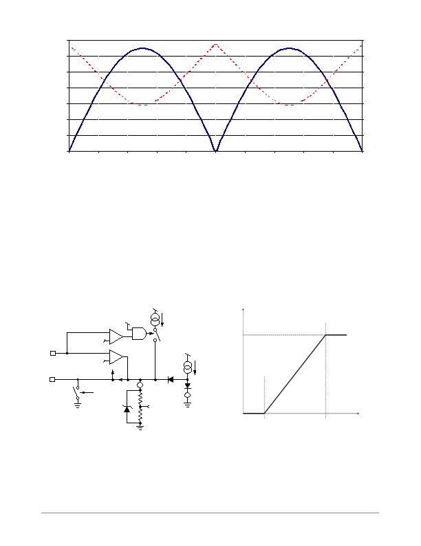
Figure 57. Input Voltage and Ontime vs Time (example with F
SW
= 100 kHz, Pin =150 W, V
AC
= 230 V, L = 200 mH)
Regulation Block and Low Output Voltage Detection
A transconductance error amplifier with access to the
inverting input and output is provided. It features a typical
transconductance gain of 200 mS and a maximum
capability of ?0 mA. The output voltage of the PFC stage
is typically scaled down by a resistors divider and
monitored by the inverting input (feedback pin Pin 4).
The bias current is minimized (less than 500 nA) to allow
the use of a high impedance feedback network. The output
of the error amplifier is pinned out for external loop
compensation (Pin 3). Typically a capacitor in the range of
100 nF, is applied between Pin 3 and ground, to set the
regulation bandwidth below 20 Hz, as need in PFC
applications.
The swing of the error amplifier output is limited within
an accurate range:
" It is forced above a voltage drop (V
F
) by some circuitry.
" It is clamped not to exceed 3.0 V + the same V
F
voltage
drop.
Hence, V
Pin3
features a 3 V voltage swing. V
Pin3
is then
offset down by (V
F
) and divided by three before it connects
to the
V
TON
processing block
and the PWM section.
Finally, the output of the regulation is a signal (
V
REGUL
of the block diagram) that varies between 0 and 1 V.
V
ref
Figure 58. Regulation Block
FB
OFF
?0 mA
OVLflag1
2R
3 V
0.955*Vref
pfcOK
200 mA
R
Figure 59. Correspondence between V
CONTROL
and V
REGUL
1 V
0 V
V
F
V
REGUL
V
CONTROL
3 V + V
F
V
control
+
+
V
F
V
out
Low
Detect
V
F
Error
Amplifier
V
REGUL
+
-
+
-
Provided the low bandwidth of the regulation loop, sharp
variations of the load, may result in excessive over and
undershoots. Overshoots are limited by the Overvoltage
Protection (see OVP section). To contain the undershoots, an
internal comparator monitors the feedback (V
Pin4
) and when
V
Pin4
is lower than 95.5% of its nominal value, it connects a
200 mA current source to speedup the charge of the
compensation capacitor (Cpin3). Finally, it is like if the
comparator multiplied the error amplifier gain by 10.
One must note that this circuitry for undershoots limitation,
is not enabled during the startup sequence of the PFC stage
but only once the converter has stabilized (that is when the
相关PDF资料 |
PDF描述 |
|---|---|
| V110A8C300BG | CONVERTER MOD DC/DC 8V 300W |
| 597D337X9020H2T | CAP TANT 330UF 20V 10% 3226 |
| V110A8C300BF3 | CONVERTER MOD DC/DC 8V 300W |
| F471K29Y5RN6UJ7R | CAP CER 470PF 1KV 10% RADIAL |
| V110A8C300BF | CONVERTER MOD DC/DC 8V 300W |
相关代理商/技术参数 |
参数描述 |
|---|---|
| NCP1605DR2G | 功能描述:功率因数校正 IC Enhanced PFC HV and Eff Standby RoHS:否 制造商:Fairchild Semiconductor 开关频率:300 KHz 最大功率耗散: 最大工作温度:+ 125 C 安装风格:SMD/SMT 封装 / 箱体:SOIC-8 封装:Reel |
| NCP1605FORWGEVB | 功能描述:电源管理IC开发工具 NCP1605 152 W FORWARD EVB RoHS:否 制造商:Maxim Integrated 产品:Evaluation Kits 类型:Battery Management 工具用于评估:MAX17710GB 输入电压: 输出电压:1.8 V |
| NCP1605LCDTVGEVB | 功能描述:BOARD EVAL NCP1605/1396 RoHS:是 类别:编程器,开发系统 >> 评估演示板和套件 系列:* 产品培训模块:Obsolescence Mitigation Program 标准包装:1 系列:- 主要目的:电源管理,电池充电器 嵌入式:否 已用 IC / 零件:MAX8903A 主要属性:1 芯锂离子电池 次要属性:状态 LED 已供物品:板 |
| NCP1606ADR2G | 功能描述:功率因数校正 IC PWR FCTR CONTROLLER RoHS:否 制造商:Fairchild Semiconductor 开关频率:300 KHz 最大功率耗散: 最大工作温度:+ 125 C 安装风格:SMD/SMT 封装 / 箱体:SOIC-8 封装:Reel |
| NCP1606APG | 功能描述:功率因数校正 IC LO CST PWR FCTR CONT RoHS:否 制造商:Fairchild Semiconductor 开关频率:300 KHz 最大功率耗散: 最大工作温度:+ 125 C 安装风格:SMD/SMT 封装 / 箱体:SOIC-8 封装:Reel |
发布紧急采购,3分钟左右您将得到回复。