- 您现在的位置:买卖IC网 > PDF目录22207 > NCP1653P (ON Semiconductor)IC CTRLR PFC CURRENT MODE 8DIP PDF资料下载
参数资料
| 型号: | NCP1653P |
| 厂商: | ON Semiconductor |
| 文件页数: | 10/19页 |
| 文件大小: | 0K |
| 描述: | IC CTRLR PFC CURRENT MODE 8DIP |
| 产品变化通告: | LTB Notification 03/Jan/2008 |
| 标准包装: | 50 |
| 模式: | 连续导电(CCM) |
| 频率 - 开关: | 90kHz ~ 110kHz |
| 电源电压: | 8.75 V ~ 18 V |
| 工作温度: | -40°C ~ 125°C |
| 安装类型: | 通孔 |
| 封装/外壳: | 8-DIP(0.300",7.62mm) |
| 供应商设备封装: | 8-PDIP |
| 包装: | 管件 |
| 其它名称: | NCP1653POS |
�� �
�
�NCP1653,� NCP1653A�
�Zin� +� in� +�
�t1� CrampVref� T� *� t1�
�VM� +� Vref� *�
�+� Vref�
�VM� Vout�
�Zin� +�
�Vref� IL� ?� 50�
�The� input� filter� capacitor� C� filter� and� the� front� ?� ended� EMI�
�filter� absorbs� the� high� ?� frequency� component� of� inductor�
�current� I� L� .� It� makes� the� input� current� I� in� a� low� ?� frequency�
�signal� only� of� the� inductor� current.�
�Iin� +� IL� ?� 50� (eq.2)�
�The� suffix� 50� means� it� is� with� a� 50� or� 60� Hz� bandwidth�
�of� the� original� I� L� .�
�From� (eq.1)� and� (eq.2),� the� input� impedance� Z� in� is�
�formulated.�
�V� T� *� t1 Vout� (eq.3)�
�Iin� T� IL� ?� 50�
�Power� factor� is� corrected� when� the� input� impedance� Z� in�
�in� (eq.3)� is� constant� or� slowly� varying� in� the� 50� or� 60� Hz�
�bandwidth.�
�(eq.6)�
�Cramp� T� T�
�From� (eq.3)� and� (eq.6),� the� input� impedance� Z� in� is�
�re� ?� formulated� in� (eq.7).�
�(eq.7)�
�Because� V� ref� and� V� out� are� roughly� constant� versus� time,�
�the� multiplier� voltage� V� M� is� designed� to� be� proportional� to�
�the� I� L� ?� 50� in� order� to� have� a� constant� Z� in� for� PFC� purpose.�
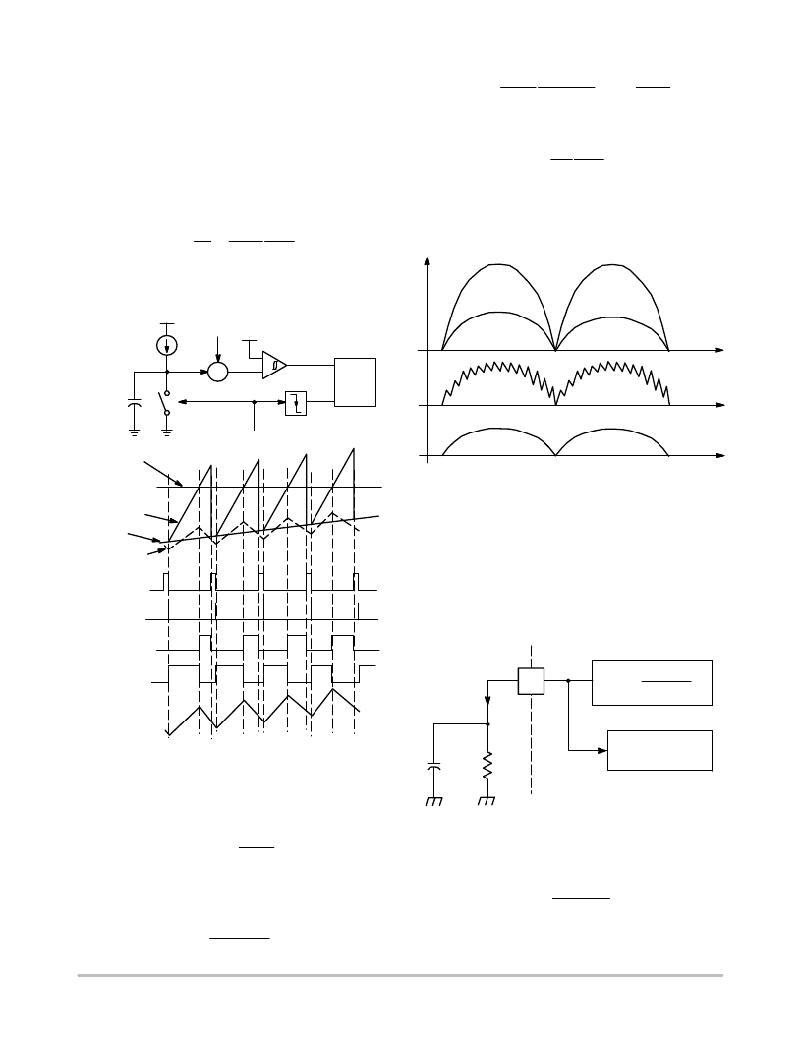
�It� is� illustrated� in� Figure� 28.�
�V� in�
�C� ramp�
�I� ch�
�0�
�1�
�V� M�
�+�
�V� re� f�
�PFC� Modulation�
�?�
�+�
�V� ramp�
�R�
�S�
�Q�
�IL�
�I� in�
�time�
�time�
�clock�
�VM�
�time�
�V� ref�
�Figure� 28.� Multiplier� Voltage� Timing� Diagram�
�V� ramp�
�V� M�
�V� M� without�
�filtering�
�Clock�
�Latch� Set�
�Latch� Reset�
�It� can� be� seen� in� the� timing� diagram� in� Figure� 27� that� V� M�
�originally� consists� of� a� switching� frequency� ripple� coming�
�from� the� inductor� current� I� L� .� The� duty� ratio� can� be�
�inaccurately� generated� due� to� this� ripple.� This� modulation�
�is� the� so� ?� called� “peak� current� ?� mode”.� Hence,� an� external�
�capacitor� C� M� connected� to� the� multiplier� voltage� V� M� pin�
�(Pin� 5)� is� essential� to� bypass� the� high� ?� frequency�
�component� of� V� M� .� The� modulation� becomes� the� so� ?� called�
�“average� current� ?� mode”� with� a� better� accuracy� for� PFC.�
�Output�
�Inductor�
�I� M�
�V� M�
�5�
�V� M� =�
�R� M� I� vac� I� S�
�2I� control�
�Current�
�Figure� 27.� PFC� Duty� Modulation� and� Timing� Diagram�
�The� PFC� duty� modulation� and� timing� diagram� is� shown�
�C� M�
�R� M�
�PFC� Duty�
�Modulation�
�Vramp� +� VM� )� ch� 1� +� Vref�
�I� t�
�VM� +�
�2� Icontrol�
�in� Figure� 27.� The� MOSFET� on� time� t� 1� is� generated� by� the�
�intersection� of� reference� voltage� V� ref� and� ramp� voltage�
�V� ramp� .� A� relationship� in� (eq.4)� is� obtained.�
�(eq.4)�
�Cramp�
�The� charging� current� I� ch� is� specially� designed� as� in�
�(eq.5).� The� multiplier� voltage� V� M� is� therefore� expressed� in�
�terms� of� t� 1� in� (eq.6).�
�Figure� 29.� External� Connection� on� the� Multiplier�
�Voltage� Pin�
�The� multiplier� voltage� V� M� is� generated� according� to�
�(eq.8).�
�RM Ivac IS�
�(eq.8)�
�Ich� +�
�Cramp Vref�
�T�
�(eq.5)�
�Input� ?� voltage� current� I� vac� is� proportional� to� the� RMS�
�input� voltage� V� ac� as� described� in� (eq.9).� The� suffix� ac�
�http://onsemi.com�
�10�
�相关PDF资料 |
PDF描述 |
|---|---|
| GSC49DREI-S734 | CONN EDGECARD 98POS .100 EYELET |
| MC33368P | IC CTRLR PFC HI VOLTAGE 16DIP |
| VE-J0W-IZ | CONVERTER MOD DC/DC 5.5V 25W |
| GMC49DREI-S734 | CONN EDGECARD 98POS .100 EYELET |
| MC33368DR2 | IC CTRLR PFC HI VOLTAGE 16SOIC |
相关代理商/技术参数 |
参数描述 |
|---|---|
| NCP1653PG | 功能描述:功率因数校正 IC Fixed Frequency Current Mode PFC RoHS:否 制造商:Fairchild Semiconductor 开关频率:300 KHz 最大功率耗散: 最大工作温度:+ 125 C 安装风格:SMD/SMT 封装 / 箱体:SOIC-8 封装:Reel |
| NCP1654BD133R2G | 功能描述:功率因数校正 IC NCP1654 - 133KHZ RoHS:否 制造商:Fairchild Semiconductor 开关频率:300 KHz 最大功率耗散: 最大工作温度:+ 125 C 安装风格:SMD/SMT 封装 / 箱体:SOIC-8 封装:Reel |
| NCP1654BD200R2G | 功能描述:功率因数校正 IC NCP1654 - 200KHZ RoHS:否 制造商:Fairchild Semiconductor 开关频率:300 KHz 最大功率耗散: 最大工作温度:+ 125 C 安装风格:SMD/SMT 封装 / 箱体:SOIC-8 封装:Reel |
| NCP1654BD65R2G | 功能描述:功率因数校正 IC NCP1654-65K-B-SOIC RoHS:否 制造商:Fairchild Semiconductor 开关频率:300 KHz 最大功率耗散: 最大工作温度:+ 125 C 安装风格:SMD/SMT 封装 / 箱体:SOIC-8 封装:Reel |
| NCP1654BP65G | 功能描述:功率因数校正 IC NCP1654-65K-B-PDIP RoHS:否 制造商:Fairchild Semiconductor 开关频率:300 KHz 最大功率耗散: 最大工作温度:+ 125 C 安装风格:SMD/SMT 封装 / 箱体:SOIC-8 封装:Reel |
发布紧急采购,3分钟左右您将得到回复。